Gas barrier film, gas barrier film manufacturing method, resin substrate for organic electroluminescent device using the aforesaid gas barrier film, and organic electroluminescent device using the aforementioned gas barrier film

a gas barrier film and manufacturing method technology, applied in the manufacture of electrode systems, synthetic resin layered products, electric discharge tubes/lamps, etc., can solve the problems of aluminum foil completely failing to meet this requirement, contents packaged in aluminum foil cannot be identified from outside, and the disposal has not yet been found, etc., to achieve excellent adhesion, high resistance to cracks, and high durability

Active Publication Date: 2011-12-08
KONICA MINOLTA INC
View PDF10 Cites 35 Cited by
  • Summary
  • Abstract
  • Description
  • Claims
  • Application Information

AI Technical Summary

Benefits of technology

[0024]The present invention provides a highly durable gas barrier film containing a compact ceramic film characterized by superb adhesion with a resin film substrate and high resistance to cracks, and a method of producing this highly durable gas barrier film, as well as a resin substrate for organic electroluminescent device, and an organic electroluminescent device by using this gas barrier film.

Problems solved by technology

However, the problem with this material is that effective method for waste disposal has not yet been found out after use, and the contents packaged in the aluminum foil cannot be identified from outside because it is basically non-transparent.
Further, transparency is very important when used as a display material, and an aluminum foil completely fails to meet this requirement.
However, since chloride-related gases are produced in the process of incineration, this material is seen as creating an environmental problem.
Further, its gas barrier function is not always satisfactory, and this material cannot be used in the field wherein a high degree of barrier function is essential.
Thus, such a film substrate as a transparent plastic is coming into use, instead of a glass substrate that is vulnerable to cracks and is difficult to increase the space.
However, the substrate such as a transparent plastic has a bas barrier function inferior to that of glass.
For example, when a substrate of inferior gas barrier function is used as a substrate of the organic electroluminescent device, the organic film will be deteriorated by permeation of vapor and air, with the result that light emitting function or durability will be lost.
Further, when a high molecular resin substrate is used as an electronic device substrate, oxygen will pass through the high molecular resin substrate to enter the electronic device, wherein oxygen will spread and deteriorate the device.
Further, the degree of vacuum required inside the electronic device cannot be maintained.
Such problems have been left unsolved.
However, despite the description of the Patent Documents 3 and 4, there are problems with the adhesion between the substrate and ceramic film (layer), and stability against chronological change in particular.

Method used


Image

  • Gas barrier film, gas barrier film manufacturing method, resin substrate for organic electroluminescent device using the aforesaid gas barrier film, and organic electroluminescent device using the aforementioned gas barrier film
  • Gas barrier film, gas barrier film manufacturing method, resin substrate for organic electroluminescent device using the aforesaid gas barrier film, and organic electroluminescent device using the aforementioned gas barrier film
  • Gas barrier film, gas barrier film manufacturing method, resin substrate for organic electroluminescent device using the aforesaid gas barrier film, and organic electroluminescent device using the aforementioned gas barrier film

Examples


example 1

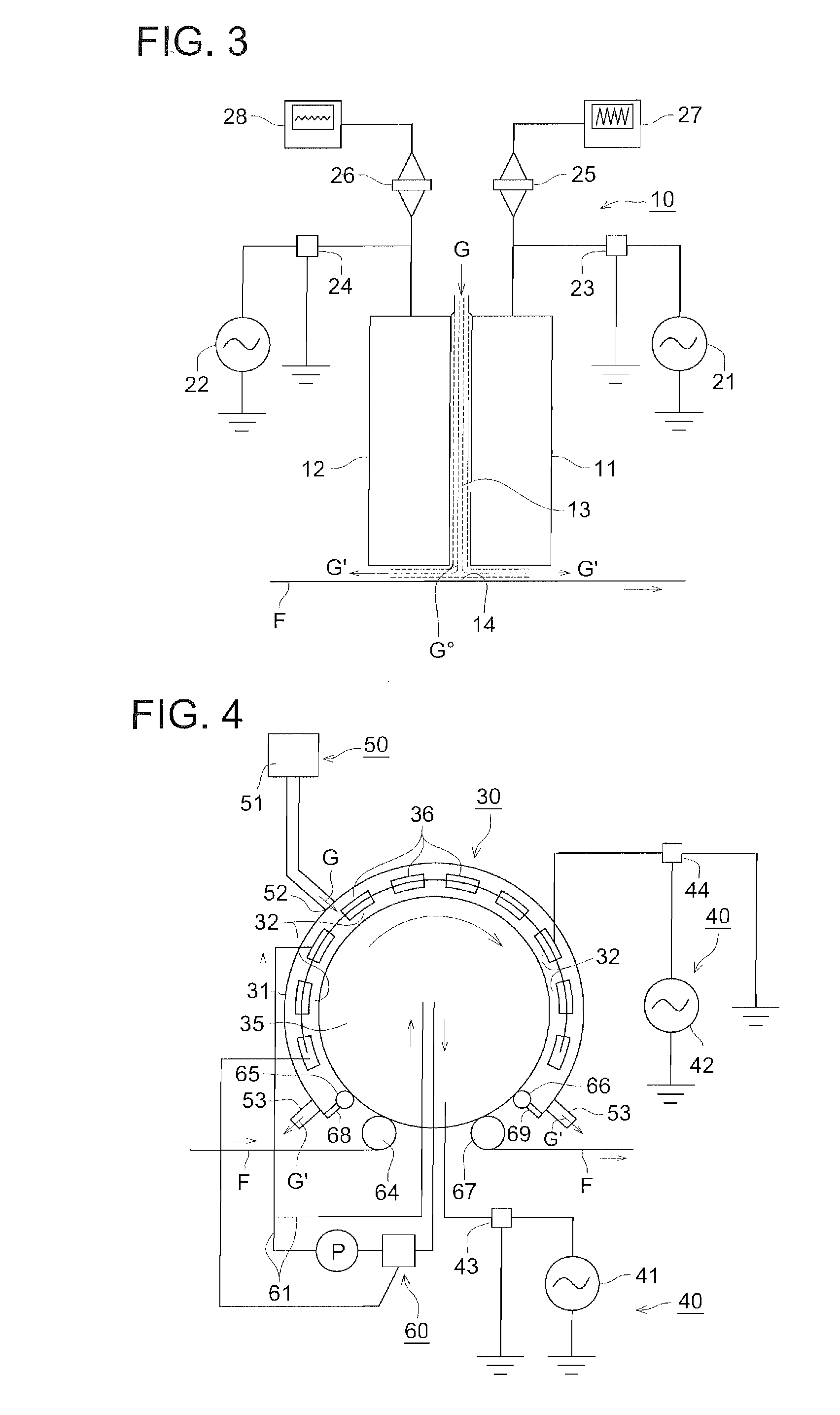
[0346]Plasma discharge processing was performed using the roll electrode type discharge processing apparatus shown in FIG. 4, and a ceramic film was formed on the substrate film. In the discharge processing apparatus, a plurality of rod-like electrodes were placed face to face with the roll electrode, parallel to the conveying direction of the film in such a way that the materials (discharge gas, reaction gas 1, 2 (to be described later)) can be supplied to each electrode.

[0347]The dielectric for coating each electrode, together with the opposing electrode, was coated on the ceramic sprayed electrode to a thickness of 1 mm on one side. After coating, the gap between the electrodes was set to 1 mm. Further, the base metal coating the dielectric was designed as a stainless steel jacket having a cooling function by coolant. Electrode temperature was controlled by coolant during the process of discharging. The light source used in this case was a high frequency power source manufactured...

example 2

[0381]A film having the following thickness was formed on the substrate according to the same procedure as that used in the Example 1, using the Model PD-270STP plasma CVD apparatus of Samco Inc.

[0382]The following describes the film forming conditions for each layer in Samples Nos. 6 through 10:

[0383]

[0384]Oxygen pressure: Gas pressure was changed at 13.3 through 133 Pa

[0385]Reaction gas: Tetraethoxy silane (TEOS), 5 sccm (standard cubic centimeter per minute)

[0386]Power: 100 W at 13.56 MHz

[0387]Retained substrate temperature: 120° C.

[0388]

[0389]The power application was reversed under the aforementioned ceramic layer film making conditions, and the substrate holding side was used as the ground. Then high frequency power was applied to the side of the opposed electrode, whereby a film was formed. The composition of the protective layer and closely bonded layer of each sample was SiO1.48C0.96. The density of the protective layer and closely bonded layer was 2.08 for the sample No. 6...

example 3

[0395]

[0396]A transparent conductive film was formed on the ceramic film of the sample No. 5 of the gas barrier film produced in the Example 1 by the following method.

[0397]A plasma discharging apparatus having parallel flat electrodes was utilized, and the aforementioned transparent film was mounted between these electrodes. Then a gas mixture was introduced to form a thin film.

[0398]In the ground electrode, the stainless steel plate measuring 200 mm×200 mm×2 mm was coated with a closely bonded alumina sprayed film. After that, the solution formed by diluting the tetramethoxy silane with ethyl acetate was coated and dried. Then it was cured by ultraviolet rays, and was provided with pore sealing treatment. Then the dielectric surface coated in this manner was polished and smoothed, and the electrode was process so that the Rmax value would be 5 μm. The applied electrode used was arranged in such a way that the hollow rectangular pure titanium pipe was coated with the dielectric und...


PUM

PropertyMeasurementUnit
thicknessaaaaaaaaaa
voltageaaaaaaaaaa
2θ/aaaaaaaaaa

Abstract

A gas barrier film comprising a resin substrate provided thereon at least one layer of a ceramic film, wherein the density ratio Y (=ρf/ρb) satisfies 1≧Y≧0.95 and the ceramic film has a residual stress being a compression stress of 0.01 MPa or more and 100 Mpa or less, wherein ρf is the density of the ceramic film and ρb is the density of a comparative ceramic film being formed by thermal oxidation or thermal nitridation of a metal as a mother material of the ceramic film so as to being the same composition ratio of the ceramic film.

Description

CROSS REFERENCE TO RELATED APPLICATIONS[0001]This Application is a Continuation of U.S. application Ser. No. 11 / 815,812, filed Aug. 8, 2007, which was a 371 of PCT / JP2006 / 302064, filed Feb. 7, 2006, which claimed the priority of Japanese Application No. 2005-040319, filed Feb. 17, 2005, the contents of each of these Applications are incorporated herein by reference.FIELD OF THE INVENTION[0002]The present invention relates to a gas barrier film mainly used as materials for packaging foods and pharmaceuticals, package for electronic devices, or as display materials of a plastic substance for organic electroluminescent device and liquid crystal; a method of manufacturing this gas barrier film; a resin substrate for organic electroluminescent device using this gas barrier film; and an organic electroluminescent device.BACKGROUND[0003]In the conventional art, a gas barrier film having a thin film of metallic oxide such as aluminum oxide, magnesium oxide and silicon oxide formed on the su...

Claims


Application Information

Patent Timeline
Patent Type & Authority Applications(United States)
IPC IPC(8): H05B33/10B32B18/00
CPCB32B15/08Y10T428/24992C04B35/14C04B35/5603C04B35/565C04B2235/77C23C16/401C23C16/505C23C16/545H01J37/32091H01J37/321H01J37/32165H01J37/32174H01L51/448H01L51/5206H01L51/5237H01L51/5271H01L51/56H01L2251/308H01L2251/5338B32B15/20B32B27/16B32B27/306B32B27/32B32B27/36B32B2255/06B32B2255/10B32B2255/205B32B2255/24B32B2307/202B32B2307/412B32B2307/422B32B2307/7242B32B2439/70B32B2439/80B32B2457/20B32B2590/00B32B27/00G02F1/133371G02F1/134363G02F2203/60B32B7/12B32B9/005B32B9/045B32B27/28B32B27/281B32B27/285B32B27/286B32B27/288B32B27/308B32B27/34B32B27/365B32B2255/20B32B2255/26B32B2307/31B32B2307/50B32B2307/514B32B2307/536B32B2307/546B32B2307/558B32B2307/702B32B2307/732B32B2457/202B32B2457/206B32B2553/00H10K30/88H10K50/81H10K50/8423H10K50/856H10K50/844H10K2102/103H10K2102/311H10K71/00
Inventor FUKUDA, KAZUHIROMAMIYA, CHIKAOARITA, HIROAKI
Owner KONICA MINOLTA INC
Why Eureka
Try Eureka