Copper base for electronic component, electronic component, and process for producing copper base for electronic component

a technology for electronic components and copper bases, applied in the direction of solid-state diffusion coatings, semiconductor/solid-state device details, coatings, etc., can solve the problems of reducing heat dissipation efficiency, forming gaps, and degrading the properties of electronic components, so as to improve plasma density and stable plasma

Inactive Publication Date: 2007-02-22
KOBE STEEL LTD
View PDF8 Cites 8 Cited by
  • Summary
  • Abstract
  • Description
  • Claims
  • Application Information

AI Technical Summary

Benefits of technology

[0061] Therefore, in applying high-frequency power to the rotating electrode, frequencies of 100 KHz or more may be used. In particular, high frequencies of 10 MHz or more is preferred. Use of high frequencies of 10 MHz or more,

Problems solved by technology

In particular, detachment disadvantageously occurs between the copper base and the resin component because of thermal stress due to a high-temperature environment, thereby forming a gap.
The formation of the gap reduces heat-dissipating efficiency when the copper base is used as a heat sink.
The formation of the gap may cause moisture absorption through the gap when the copper base is used as a lead frame, thereby degrading the properties of the electronic component, in some cases.
In this case, a gap is formed between the semiconductor element and the heat sink because of thermal stress generated in subjecting the resulting BGA package t

Method used


Image

  • Copper base for electronic component, electronic component, and process for producing copper base for electronic component
  • Copper base for electronic component, electronic component, and process for producing copper base for electronic component
  • Copper base for electronic component, electronic component, and process for producing copper base for electronic component

Examples


examples 1 to 11

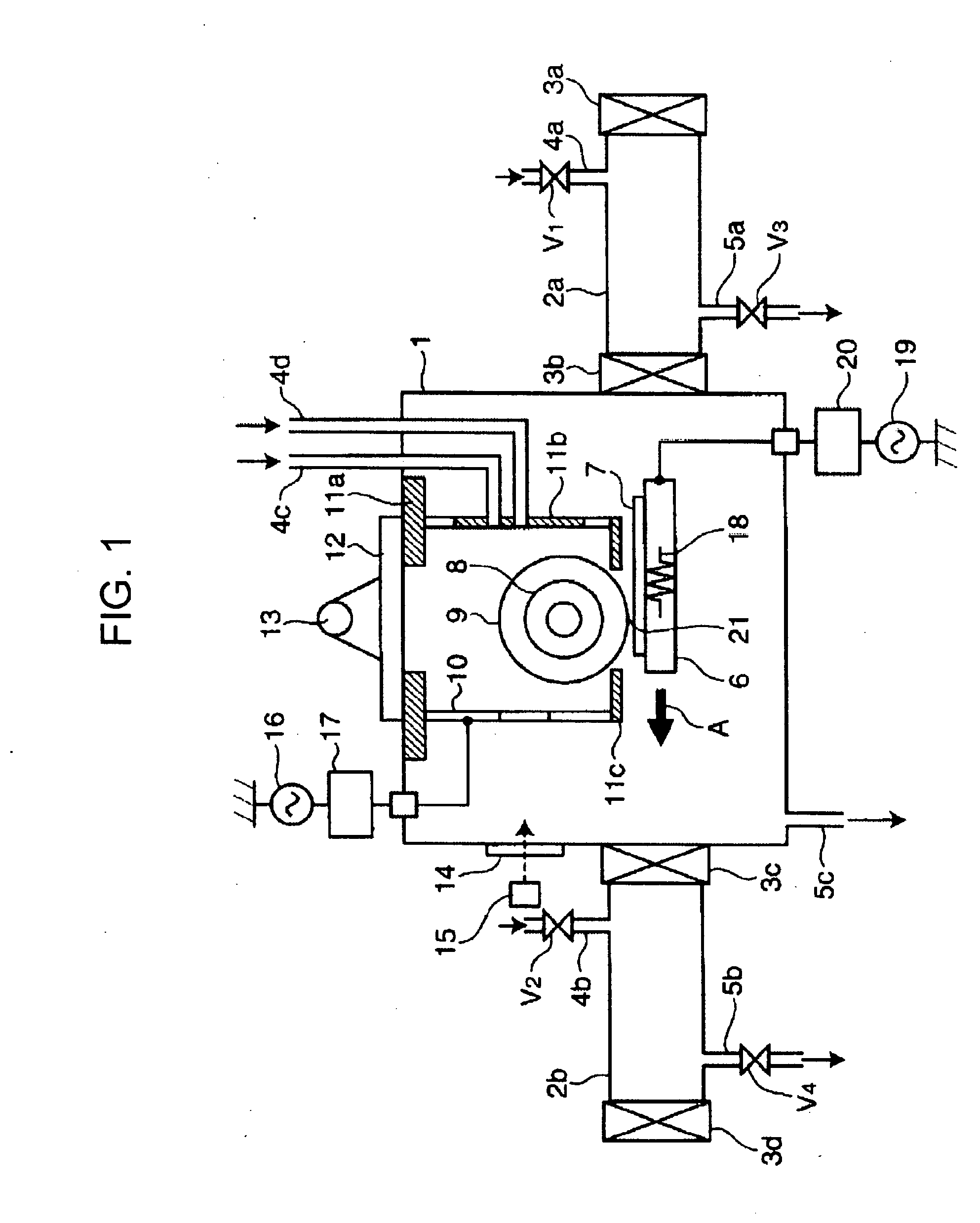
[0091] A silicon oxide thin film was formed with the film-forming apparatus by CVD shown in FIG. 1, the apparatus including a rotating electrode.

[0092] In the figure, the base holder 6 having a width of 170 mm and a length (length in the transfer direction) of 170 mm was used. The base 7 was placed on the base holder 6 and then placed in the chamber 1.

[0093] The base 7 had a width of 100 mm, a length (length in the transfer direction) of 150 mm, and a thickness of 0.4 mm and was composed of a copper alloy having a composition of Cu-0.1 percent by mass of Fe-0.03 percent by mass of P (C19210), the copper alloy being plated with Ni or a Ni alloy.

[0094] After the front end of the base holder 6 was transferred to a position directly below the rotating electrode 9, radio-frequency power (13.56 MHz, 500 W) was applied from the radio-frequency power source 16 to the rotating electrode 9. The base holder 6 was grounded.

[0095] The temperature of the base holder 6 was set at 100° C. to 25...

examples 12 to 23

[0108] Samples were prepared and evaluated as in EXAMPLES 1 to 11, except that when the thicknesses of the silicon oxide thin films were 20, 40, 250, and 500 nm, oxygen was added such that the partial pressure of oxygen was 0.1 to 2 times that of TEOS (0.133 to 2.66 kPa). Table 2 shows the results.

TABLE 2EXAMPLE121314151617Thin film-Partial pressure of TEOS0.13330.13330.13330.26660.26660.2666forming(kPa)conditionsPartial pressure of Helium101.18101.06100.92101.03100.79100.52(kPa)Partial pressure of oxygen0.01330.13330.26660.02670.26660.5333(kPa)Total pressure (kPa)101.32101.32101.32101.32101.32101.32Partial pressure of oxygen / partial0.1120.112pressure of TEOSTemperature of base200200200200200200holder (° C.)Thickness (nm)202020404040Die shear strength (room temperature) (MPa)17.65211.76814.7111.76815.69117.652EXAMPLE181920212223Thin film-Partial pressure of TEOS0.93330.93330.93332.66642.66642.6664forming(kPa)conditionsPartial pressure of Helium100.399.45898.52598.63295.99293.325(k...

example 24

[0109] Sample was prepared as in EXAMPLES 1 to 11, except that the film-forming temperature was set at 100° C. As a result, the migration of active species generated by plasma decomposition was suppressed on the surface to form irregularities on the surface. The thickness was set at 200 nm. The resulting film was evaluated on the surface morphology with an atomic force microscope (AFM). It was conformed that the peak-to-valley (P-V) height of a surface was 1 μm or less. The die shear strength was 22 MPa. That is, the die shear strength was significantly increased.


PUM

PropertyMeasurementUnit
Thicknessaaaaaaaaaa
Surface roughnessaaaaaaaaaa
Pressureaaaaaaaaaa

Abstract

A copper base for an electronic component includes a silicon oxide thin film containing at least one of a hydrocarbon group and a hydroxy group is used, the silicon oxide thin film being disposed on a surface of the copper base. Furthermore, a silicon-containing reaction gas is decomposed by generating plasma. The resulting decomposition product is brought into contact with the copper base to form a silicon oxide thin film on a surface of the copper base.

Description

BACKGROUND OF THE INVENTION [0001] 1. Field of the Invention [0002] The present invention relates to a copper base for an electronic component for use in an electronic component such as a semiconductor device. The present invention also relates to an electronic component including the copper base. Furthermore, the present invention relates to a method for forming a silicon oxide thin film suitable for producing the copper base for the electronic component. Specifically, the present invention relates to a copper base for an electronic component, the base having improved adhesion to a resin adhesive and a resin sealant. The present invention also relates to an electronic component including the copper base for the electronic component. Furthermore, the present invention relates to a method for forming a silicon oxide thin film suitable for producing the copper base for the electronic component. [0003] 2. Description of the Related Art [0004] Copper or copper-alloy bases, as needed, th...

Claims


Application Information

Patent Timeline
IPC IPC(8): C23C16/40C23C16/513
CPCC23C16/401H01L23/3142H01L23/49586H01L2924/1433H01L2924/19041H01L2924/0002H01L2924/3011H01L2924/00
Inventor HAYASHI, KAZUSHIKUGIMIYA, TOSHIHIRO
Owner KOBE STEEL LTD
Why Eureka
Try Eureka