Electrical or electronic composite component and method for producing an electrical or electronic composite component

a technology of composite components and components, applied in the direction of paper/cardboard containers, semiconductor/solid-state device details, containers, etc., can solve the problems of increased crack formation, limited reliability, and high volume of gas exchange, and achieve the effect of low cost and reproducibility

Inactive Publication Date: 2011-12-15
ROBERT BOSCH GMBH
View PDF6 Cites 11 Cited by
  • Summary
  • Abstract
  • Description
  • Claims
  • Application Information

AI Technical Summary

Benefits of technology

[0005]The exemplary embodiments and / or exemplary methods of the present invention are based on the object of proposing an electronic or electrical composite component, as well as a manufacturing method for such a composite component, in which crack formation during joining can be avoided. The composite component may be producible at low cost, and reliable under the stress of changes of temperature.
[0007]An important aspect of the exemplary embodiments and / or exemplary methods of the present invention is to join at least two joining partners to one another not directly using sintering paste, as in the prior art, i.e. fixing them solidly together, but rather to connect the joining partners fixedly without using sintering paste, using a previously produced sintered compact having continuous open porosity. The thickness of the sintered compact (sintered foil) that is used may be between approximately 10 μm and approximately 300 μm or more in the direction of stacking of the joining partners. Such a sintered compact has the advantage of gas channels that are already integrated and that are stable in the following process of joining to the joining partners, for the aeration and de-aeration of the joining points that are formed for example by soldering, welding, or gluing. The use of a porous sintered compact as an insert or intermediate part has a positive effect on the joining process for joining the joining partners to the sintered compact, in particular if joining partners having large surfaces, such as silicon power semiconductors and circuit substrates, or circuit substrates and heat sinks, are to be joined to the sintered compact. It is also possible to connect punched grids via a sintered compact. A further advantage of the use of a sintered compact is that it provides more freedom in the design of the joining point, because the sintered compact can have a larger surface than at least one of the joining partners, which may be than both the joining partners, and / or the joining partners can be situated significantly further from one another than is possible in the process controlling according to the prior art, i.e. given an immediate sintering of the joining partners using sintering paste. In particular, the advantage is an increased ability to withstand changes in temperature.
[0012]Alternatively, it is possible to solder at least one joining partner, which may be both joining partners, to the sintered compact, which may be done by using soldering paste, soldering powder, or a solder perform (generally: soldering material). Here, due to the action of temperature the soldering material enters a liquid phase and binds the sintered compact to the at least one joining partner. Quite particularly, the soldering material may be lead-free soldering paste, but it is also conceivable to use soldering pastes containing lead, in particular standard soldering pastes. Due to its porous structure, the sintered compact that is used is highly suitable for entering into a robust soldering bond. This is due above all to the good wettability of the sintered compact with all standard soldering materials, in particular if the sintered compact is made at least partly of silver metal, in particular silver metal flakes. The “buffering” effect of the sintered compact significantly reduces the destructive effect that thermomechanical tensions have on the pure soldering material, in particular during the later use of the electrical or electronic composite component. The soldering material that is used, in particular soldering paste, may be either applied, in particular pressed on or dispensed, both to the joining partners and to the sintered compact, which then acts as a depot, or alternatively is applied only to both sides of the sintered compact, or, as a further alternative, is applied only to one side of the sintered compact and to only one joining partner. The gases that arise during the soldering process can optimally be carried off through the gas channels formed by the porosity of the sintered compact. It is also possible, in a soldering paste pressure process carried out before the actual soldering process, to apply a solder depot to the later joining points for the fitting of SMD components and subsequent reflow soldering. In this case, it is necessary merely to further apply flux to these points. The porous structure of the sintered compact provides sufficient possibilities for the degassing of the flux system.
[0017]The exemplary embodiments and / or exemplary methods of the present invention is also directed to a method for producing an electrical or electronic composite component, which may be a composite component fashioned as described above. The core of the method is to connect at least two joining partners to a sintered part (sintered foil) having open porosity, which may be by immediate sintering without using sintering paste, by soldering using a soldering material, in particular lead-free soldering material, which may be soldering paste, by gluing, in particular conductive gluing, which may be done using a glue containing silver, or alternatively by welding, in particular frictional welding, ultrasound welding, or resistance welding. The advantage of the method according to the present intention is that the continuous open porosity of the structure of the sintered compact allows gases to escape during the process of connecting to the joining partners, and as needed gases such as oxygen can be conducted to the joining points so that crack formation is avoided. The conducting away of gas and the supply of gas may take place from the lateral direction, i.e. transverse to the stacking direction of the joining partners.

Problems solved by technology

Lead-free soft solder alloys based on SnAgCu may be used as substitute alloys only to a certain extent, because these are limited in their reliability, in particular under passive and active temperature change stress.
When the process is carried out using sintering paste, there is the difficulty that high volumes of gas have to be exchanged through the sintering layer; thus, oxygen must reach the joining points, and the solvents, as well as combusted / oxidized organic materials, must be able to exit.
In particular at the desired low process pressures, this results in an increased formation of cracks, in particular given joining over large surfaces.

Method used


Image

  • Electrical or electronic composite component and method for producing an electrical or electronic composite component
  • Electrical or electronic composite component and method for producing an electrical or electronic composite component
  • Electrical or electronic composite component and method for producing an electrical or electronic composite component

Examples


Embodiment Construction

[0023]In the Figures, identical elements, and elements having identical function, are identified by the same reference characters.

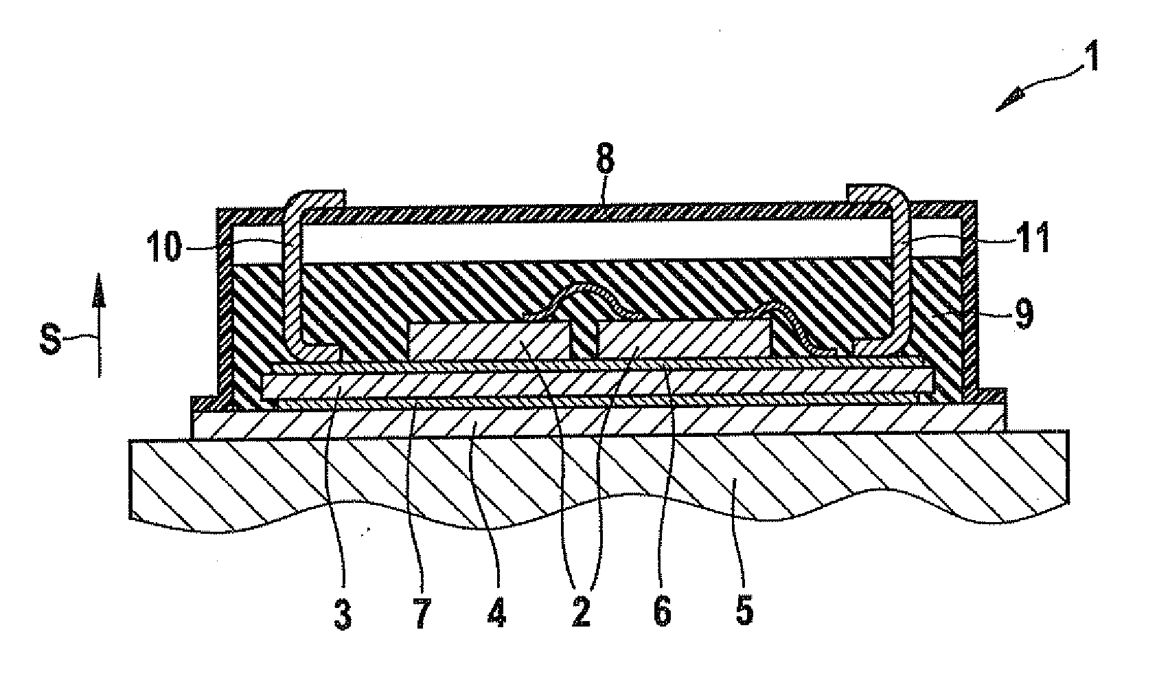
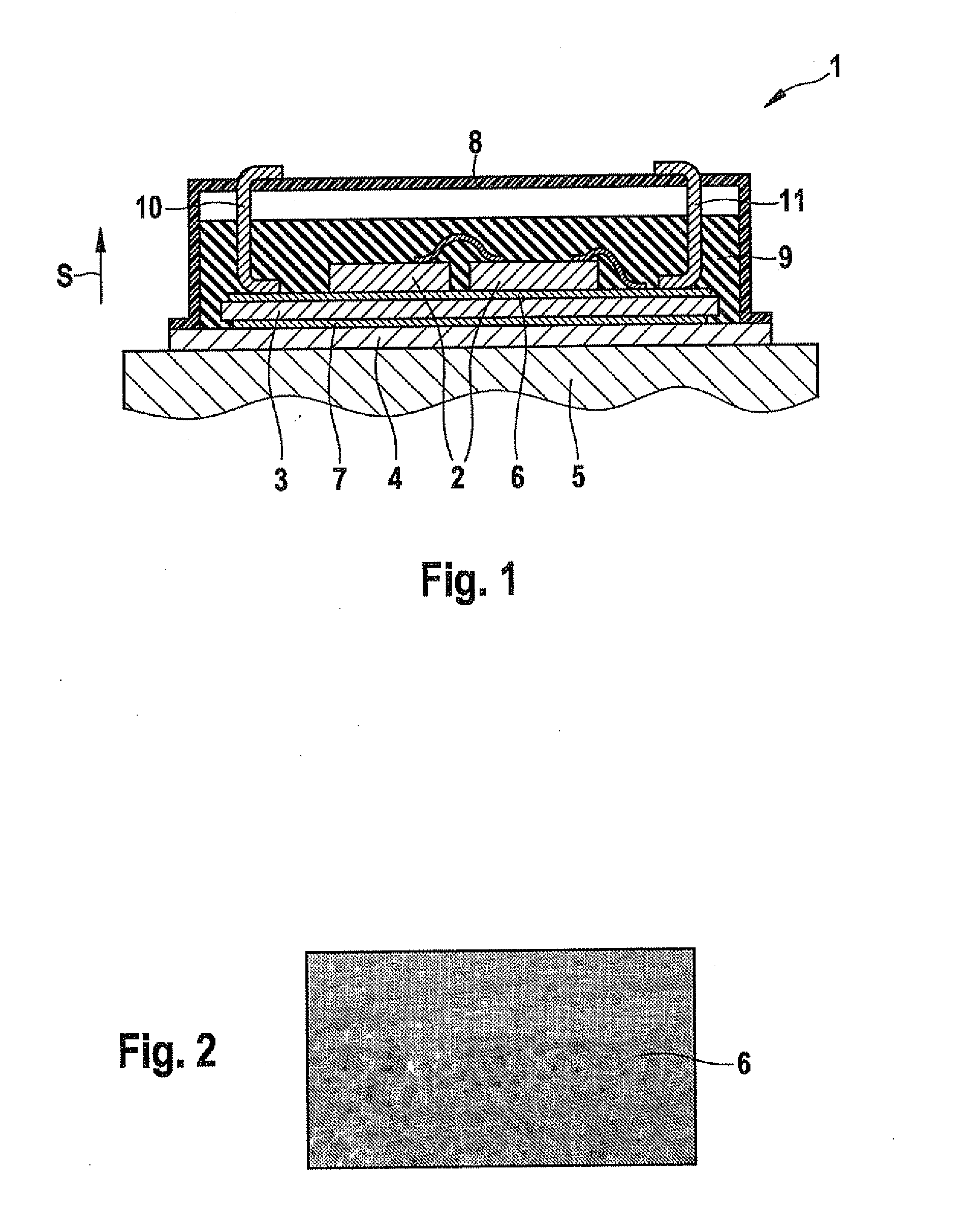
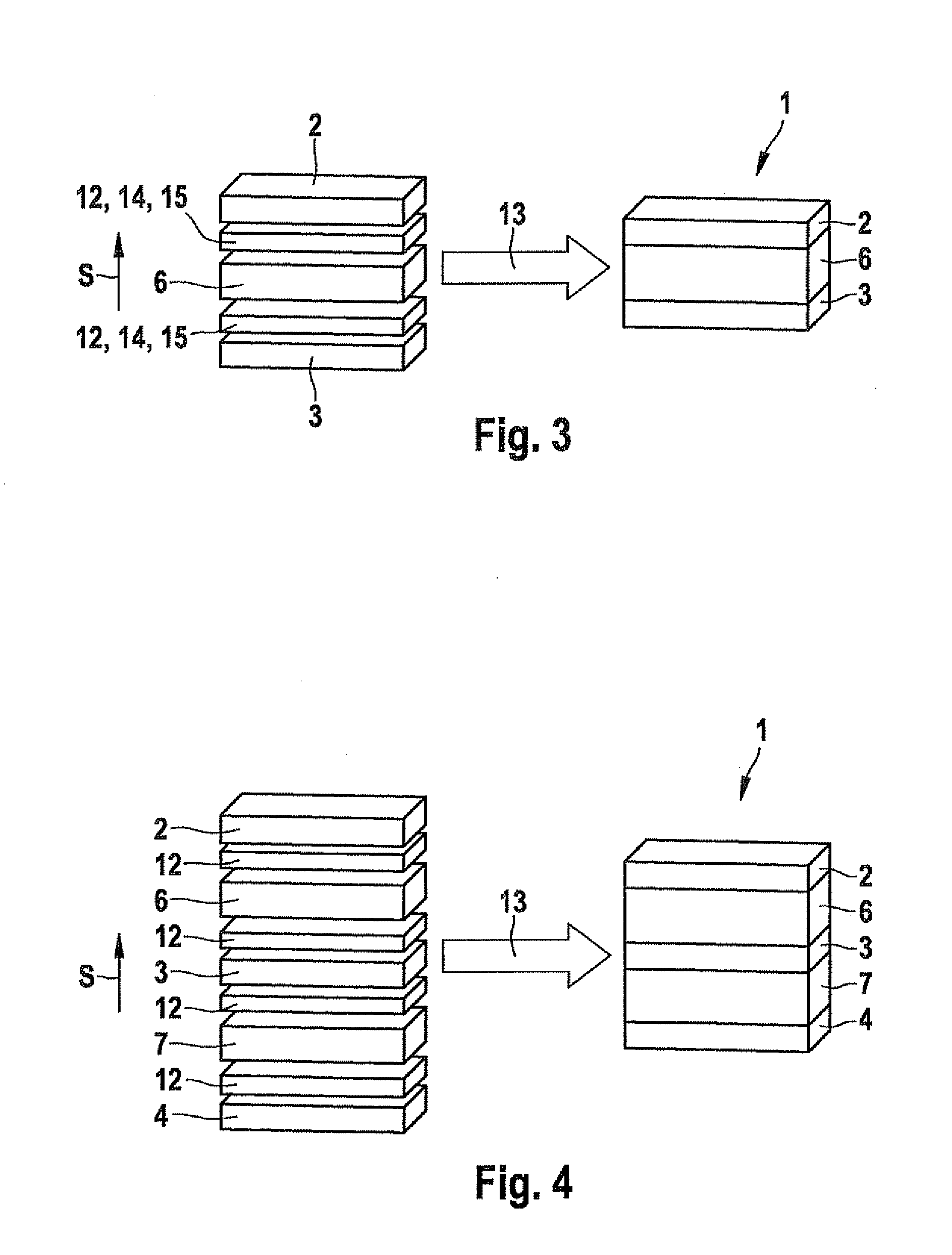
[0024]FIG. 1 shows an electronic composite component 1. This component has a first joining partner 2, a second joining partner 3, and a third joining partner 4. In the depicted exemplary embodiment, first joining partner 2 is a power semiconductor component, here an 1 GB transistor. Second joining partner 3 is a circuit substrate, and third joining partner 4 is a base plate made of copper. The base plate made of copper is in turn fixed to a cooling element 5 (heat sink).

[0025]Between first joining partner 2 and second joining partner 3 there is situated a sintered compact 6 having a thickness of approximately 5 μm in a stack direction S. First joining partner 2 and second joining partner 3 are fixed to two oppositely situated sides of sintered compact 6, in each case by soldering using soldering paste (or, alternatively, for example soldering powder or a ...


PUM

PropertyMeasurementUnit
temperatureaaaaaaaaaa
pressureaaaaaaaaaa
pressureaaaaaaaaaa

Abstract

An electrical or electronic composite component is described as having a first joining partner and at least one second joining partner. According to the present system, it is provided that a sintered compact having open porosity is accommodated between the first and the second joining partner, the sintered compact is connected fixedly to the first and to the second joining partner.

Description

FIELD OF THE INVENTION[0001]The present invention relates to an electrical or electronic composite component, and to a method for producing an electrical or electronic composite component.BACKGROUND INFORMATION[0002]The joining of power semiconductors, such as JFETs, MOSFETs, IGBTs, or diodes, to a circuit substrate of a power electronics assembly, and also the joining of the circuit substrate to a baseplate / heat sink, are typically realized using soft solder technology. Based on new EU regulations, in the future the use of soft solder alloys containing lead (Sn63Pb37 and Sn5Pb95) is to be forbidden. Lead-free soft solder alloys based on SnAgCu may be used as substitute alloys only to a certain extent, because these are limited in their reliability, in particular under passive and active temperature change stress. Alternative high-melting-paint soft solders used as substitute alloys are either too brittle to handle (Bi97, 5Ag2.5) or are too expensive (Au80Sn20).[0003]The immediate s...

Claims


Application Information

Patent Timeline
Patent Type & Authority Applications(United States)
IPC IPC(8): H05K7/20B32B37/02B32B37/14B32B37/10B32B37/12H05K13/00B32B37/06
CPCH01L23/3735Y10T156/10H01L2224/48137H01L2224/48227H01L2224/48472H01L2224/48091H01L2924/1305H01L2924/13062H01L2924/1461H01L2924/12041H01L2224/29339H01L2924/13055H01L2924/13091H01L2224/2908H01L2224/8384H01L24/48H01L2924/00014H01L2924/00H01L2224/83205H01L2924/12042H01L2924/181H01L2224/83101H01L2924/00012H01L2224/45099H01L2224/45015H01L2924/207
Inventor RITTNER, MARTINPETER, ERIKGUENTHER, MICHAEL
Owner ROBERT BOSCH GMBH
Why Eureka
Try Eureka