Supercharge Your Innovation With Domain-Expert AI Agents!

Optical modulation structure and optical modulator

a technology of optical modulation and optical modulator, which is applied in the direction of optics, optical waveguide light guide, instruments, etc., can solve the problems of canceling the original electrooptic effect and many devices examined so far in poor optical modulation efficiency

Active Publication Date: 2011-12-22
NEC CORP
View PDF6 Cites 12 Cited by
  • Summary
  • Abstract
  • Description
  • Claims
  • Application Information

AI Technical Summary

Benefits of technology

The present invention relates to an optical modulation structure and an optical modulator that can quickly convert a high-speed electrical signal into an optical signal using silicon. The invention aims to solve the problem of low optical modulation efficiency and the need for a high-speed optical switch or modulator for use in more optical communication systems. The invention proposes a new electrooptic modulator that can change the refractive index using the carrier plasma effect, resulting in a higher optical modulation efficiency and shorter optical phase modulation length. The invention also describes a new structure for the electrooptic phase modulator that allows for higher integration and lower power consumption.

Problems solved by technology

However, many of the devices examined so far are poor in the optical modulation efficiency and require a length of mm order for optical phase modulation and an injection current density higher than 1 kA / cm3.
For this reason, the refractive index change in the silicon layer caused by the thermooptic effect may problematically cancel the original electrooptic effect.

Method used


Image

  • Optical modulation structure and optical modulator
  • Optical modulation structure and optical modulator
  • Optical modulation structure and optical modulator

Examples


first exemplary embodiment

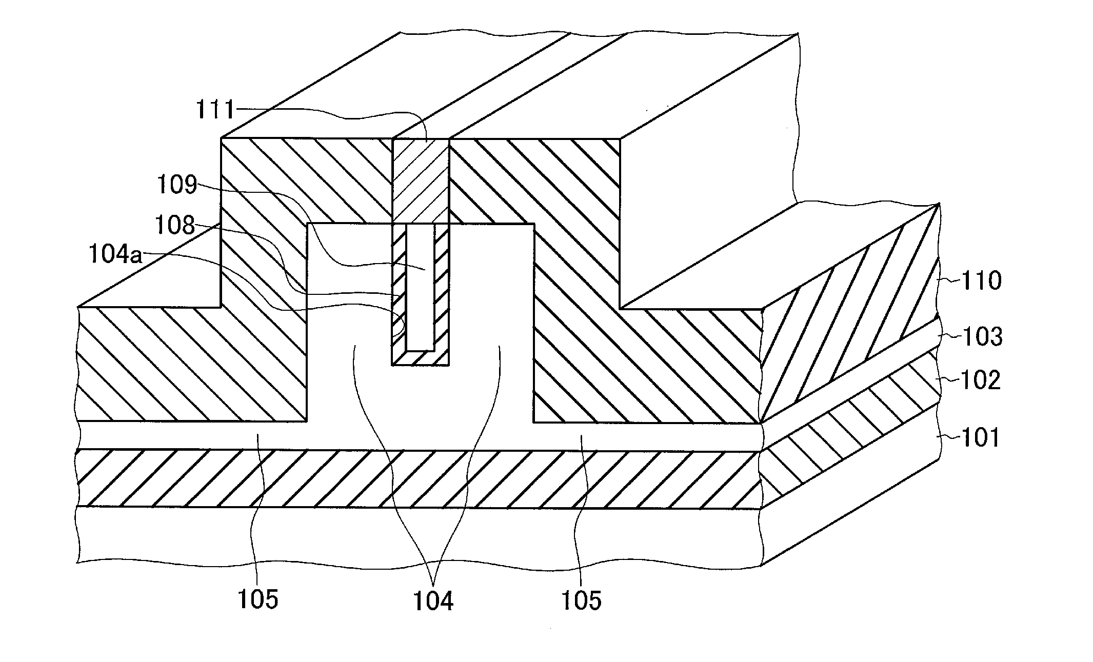
[0045]The first exemplary embodiment will be described first with reference to FIGS. 1 and 2. FIG. 1 is a perspective view showing the arrangement of an optical modulator according to the first exemplary embodiment. FIG. 1 illustrates a section, too. FIG. 2 is a plan view.

[0046]The optical modulation structure of this exemplary embodiment includes a lower cladding layer 102, a first silicon layer 103 integrally formed from silicon of a first conductivity type on the lower cladding layer 102 while including a core 104 and slab regions 105 arranged on both sides of the core 104 and connected to the core, a concave portion 104a formed in the upper surface of the core 104, and a second silicon layer 109 of a second conductivity type formed on a dielectric layer 108 in the concave portion 104a so as to fill the concave portion 104a. The core 104 includes the dielectric layer 108 and the second silicon layer 109 which are formed in the concave portion 104a. Note that in this exemplary emb...

second exemplary embodiment

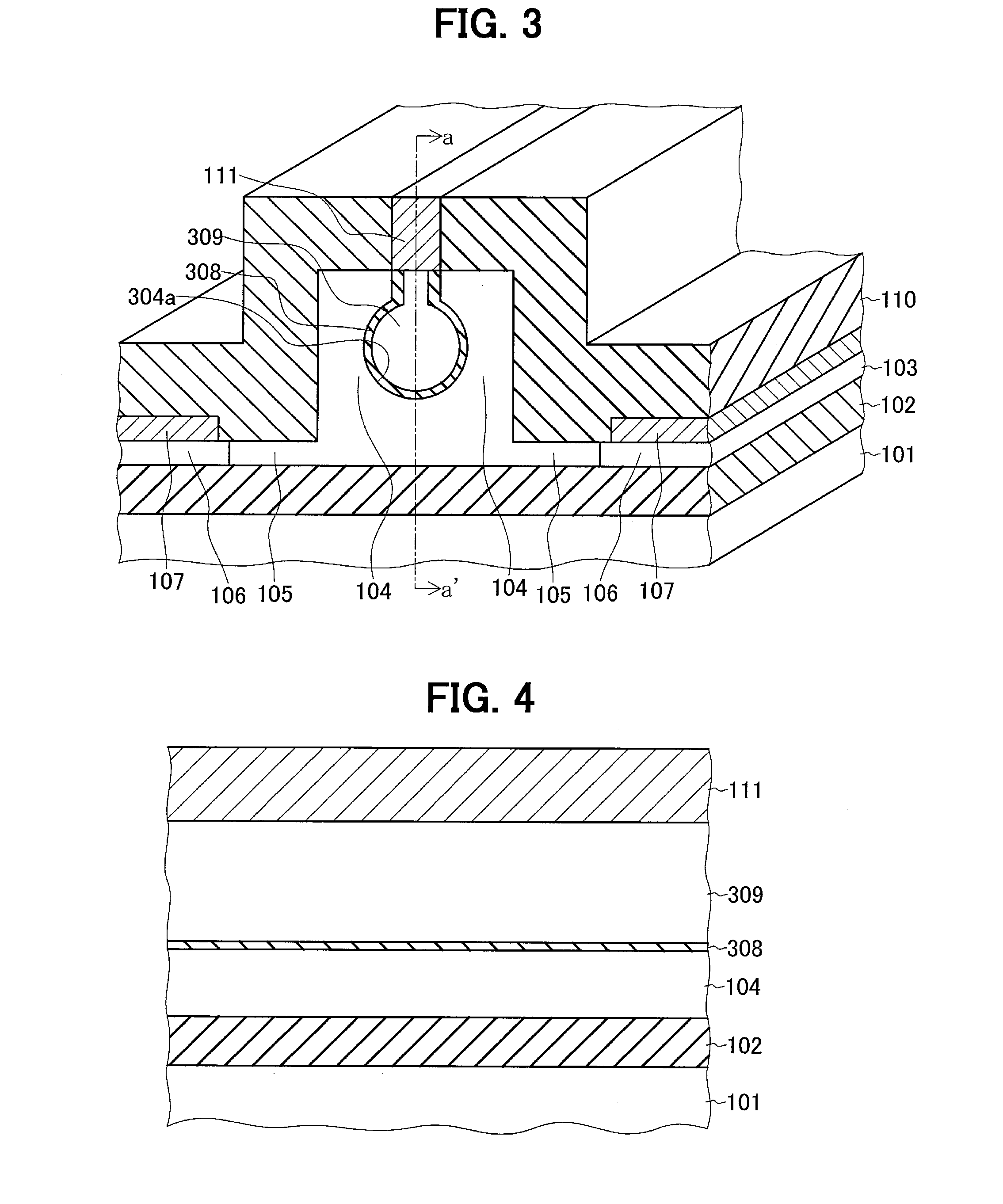
[0069]The second exemplary embodiment will be explained next with reference to FIGS. 3 and 4. FIG. 3 is a perspective view of the second exemplary embodiment, and illustrates a section, too. In this exemplary embodiment, a concave portion 304a formed from the upper surface of a core 104 has a central region where the opening is wider than that of the upper portion of the core 104, and the sidewall of the central region is curved. FIG. 3 illustrates a section of the concave portion 304a including a rectangular portion on the upper side and a circular portion on the lower side. Hence, the section of a second silicon layer 309 of a second conductivity type formed on a dielectric layer 308 also includes a rectangular portion on the upper side and a circular portion on the lower side. In this exemplary embodiment as well, the core 104 includes the dielectric layer 308 and the second silicon layer 309 which are formed in the concave portion 304a.

[0070]This can make the region where the d...

third exemplary embodiment

[0075]The third exemplary embodiment will be described next with reference to FIGS. 5 and 6. FIGS. 5 and 6 are sectional views showing the arrangement of an optical modulation structure according to the third exemplary embodiment. FIG. 6 shows a section taken along a line b-b′ in FIG. 5.

[0076]In this exemplary embodiment, a plurality of concave portions 504a are provided in a core 104. In each concave portion 504a, a second silicon layer 509 is formed on a dielectric layer 508 to fill the concave portion. A plurality of first electrode extraction portions 511 are formed on the core 104 and connected to the second silicon layers 509, respectively. The plurality of concave portions 504a are arrayed in the running direction of the core 104 (light propagation direction) while being spaced apart from each other. In this exemplary embodiment, the plurality of concave portions 504a are arrayed at equal intervals.

[0077]In this exemplary embodiment, each concave portion 504a has a central re...


PUM

PropertyMeasurementUnit
communication wavelengthaaaaaaaaaa
thicknessaaaaaaaaaa

Abstract

The components are a lower clad layer (102), a first silicon layer (103) that is formed on the lower clad layer (102) as a single body made of silicon of a first conduction type and has a slab region (105) that is disposed at a core (104) and on both sides of the core (104) and connects to the core, a concave section (104a) that is formed in the top surface of the core (104), and a second silicon layer (109) of a second conduction type that is formed inside the concave section (104a) with an intervening dielectric layer (108) to fill the inside of the concave section (104a).

Description

TECHNICAL FIELD [0001]The present invention relates to an optical modulation structure and an optical modulator which are required in the information processing and communication fields to quickly convert a high-speed electrical signal into an optical signal using silicon.BACKGROUND ART[0002]There are used silicon-based optical communication devices having an optical fiber communication wavelength of 1330 or 1500 nm for various systems such as home optical fibers and local area networks (LANs). The silicon-based optical communication device is a very promising technique that allows to integrate optical functional elements and electronic circuits on a silicon platform using the CMOS technology.[0003]In recent years, silicon-based passive devices such as a waveguide, an optical coupler, and a wavelength filter have been studied very widely. In addition, silicon-based active elements such as an optical modulator and an optical switch have received a great deal of attention as an import...

Claims


Application Information

Patent Timeline
Patent Type & Authority Applications(United States)
IPC IPC(8): G02F1/025
CPCG02F1/025
Inventor FUJIKATA, JUNICHIUSHIDA, JUNTODA, AKIOSAITOH, MOTOFUMI
Owner NEC CORP
Features
  • R&D
  • Intellectual Property
  • Life Sciences
  • Materials
  • Tech Scout
  • Unparalleled Data Quality
  • Higher Quality Content
  • 60% Fewer Hallucinations
Learn More