

Two-layer flexible substrate, and copper electrolytic solution for producing same
a flexible substrate and flexible technology, applied in the direction of crystal growth process, core/yokes, transportation and packaging, etc., can solve the problems of wiring line size reduction, method involves a complex process, and wiring defects
Inactive Publication Date: 2011-12-22
JX NIPPON MINING& METALS CORP
View PDF1 Cites 13 Cited by
- Summary
- Abstract
- Description
- Claims
- Application Information
AI Technical Summary
Benefits of technology
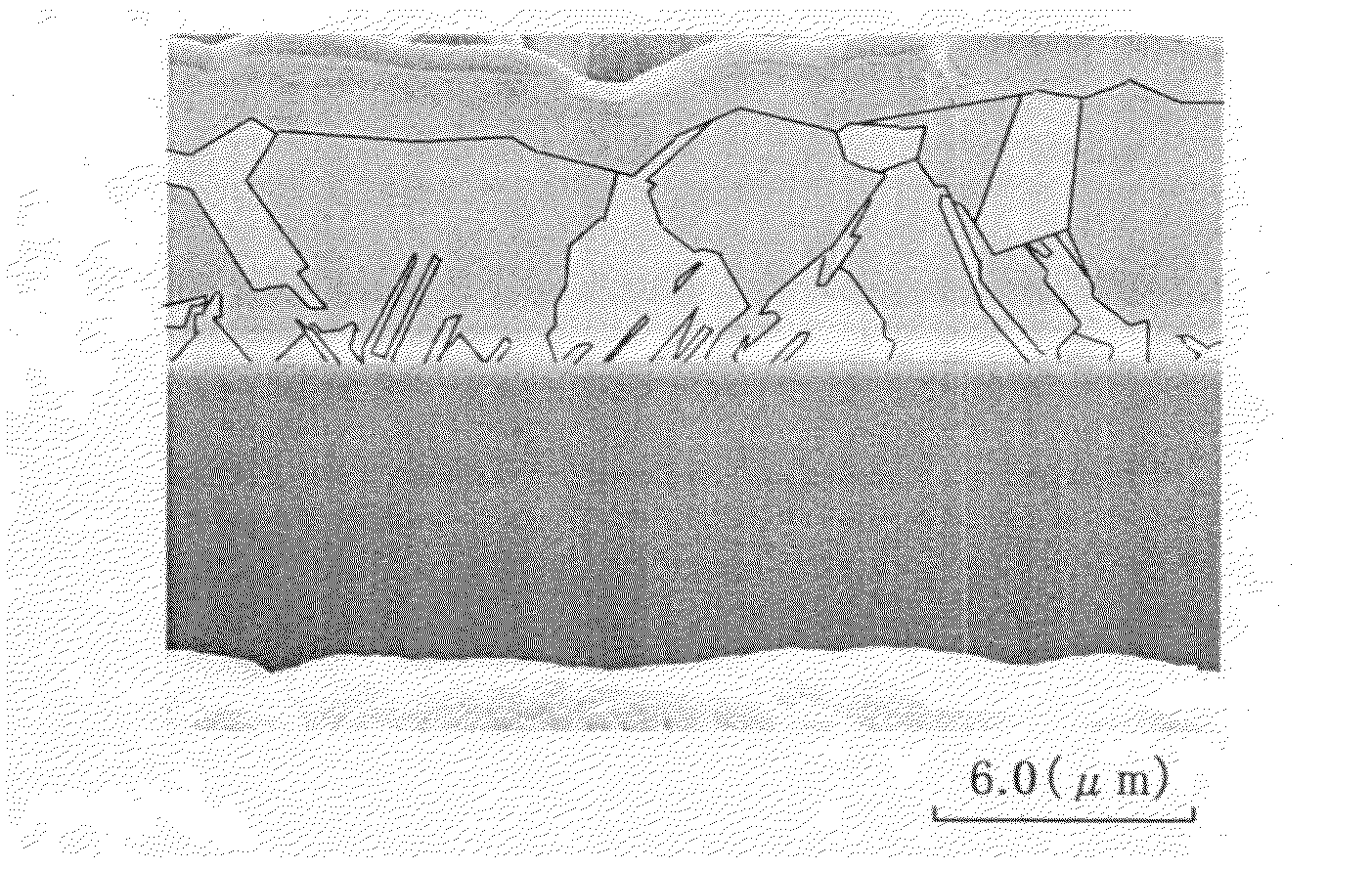
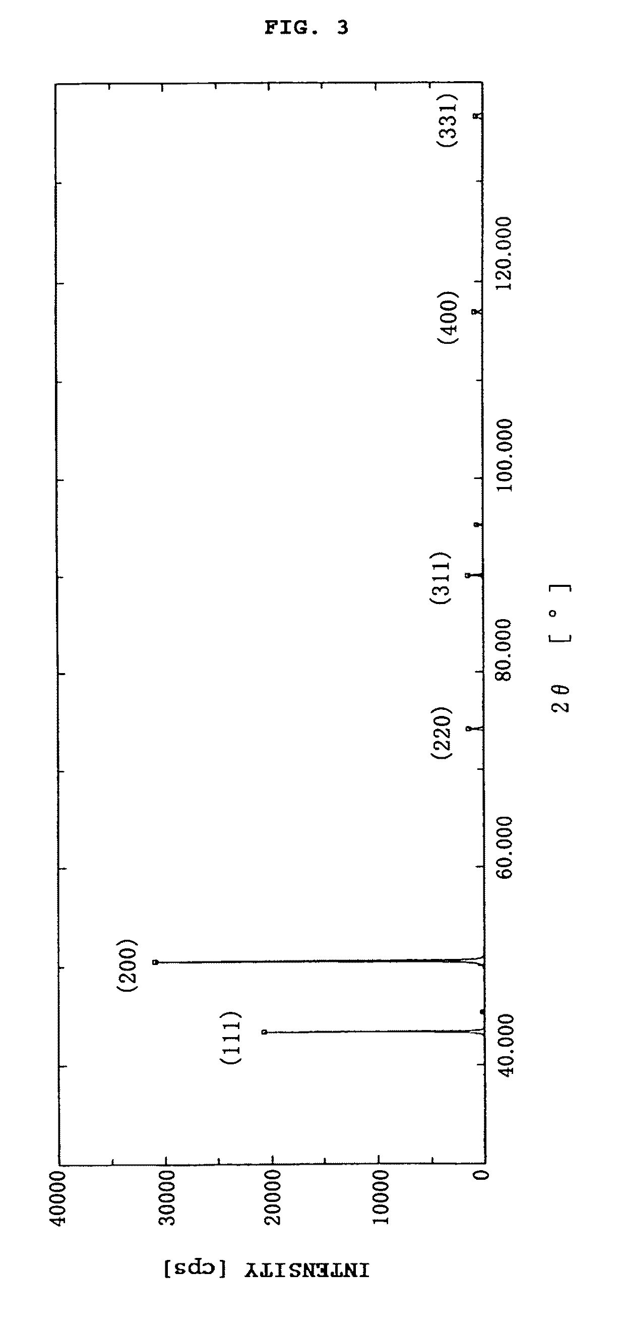
[0020]In the two-layer flexible substrate fabricated using the copper electrolytic solution in accordance with the present invention, the average size of copper crystal grains constituting the copper layer is made equal to or greater than 1 μm and equal to or less than the thickness of the copper layer, and a ratio of peak intensity of (200) to a sum total of intensities of six principal peaks in the X-ray diffraction of the copper layer is made equal to or greater than 0.4, thereby making it possible to obtain an MIT property of equal to or greater than 300 times. Further, when a heat treatment is performed during wiring, no Kirkendall voids occur.
Problems solved by technology
However, a large number of pinholes are formed and exposed portions of the insulating film are thereby created in the underlying metal layer thus obtained, and when a thin-film copper conductor layer is provided, the exposed portions created by pinholes cannot be filled with copper and pinholes also appear on the copper conductor layer surface, thereby causing wiring defects.
However, this method involves a complex process.
In particular, in recent years, the number of pins and lead portions (connection portions (inner leads, outer leads) of COF (Chip on film) in two-layer flexible substrates has increased, the line / space (the width of a line and the width of a space, or a combined width of line and space) has decreased, the wiring lines have decreased in size, and the probability of breakage during folding performed when the COF is mounted has increased.
Where fine crystals with a crystal grain size of about several hundreds of nanometers are present in a copper layer, when the heat treatment is performed, voids called Kirkendall voids appear due to a difference in diffusion rate between copper and tin, and the tin film peels off, thereby causing a short circuit.
Method used
View moreImage
Smart ImageViewing Examples

Examples
example
[0048]The present invention will be explained below on the basis of examples thereof, but the present invention is not limited to the examples.
Login to View More PUM
| Property | Measurement | Unit |
|---|---|---|
| thickness | aaaaa | aaaaa |
| temperature | aaaaa | aaaaa |
| size | aaaaa | aaaaa |
Abstract
It is an object of the invention to provide a two-layer flexible substrate that excels in folding endurance and free from occurrence of Kirkendall voids or the like even when lead portions of COF are plated with tin and heat treatment is performed. The present invention is directed to a two-layer flexible substrate in which a copper layer is provided on one or both faces of an insulating film by using a copper electrolytic solution, wherein an average size of copper crystal grains constituting the copper layer is equal to or greater than 1 μm and equal to or less than a thickness of the copper layer, and a ratio of peak intensity of (200) to a sum total of intensities of six principal peaks {[peak intensity of (200)] / [sum total of peak intensities of (111), (200), (220), (311), (400), (331)]} in the X-ray diffraction of the copper layer is equal to or greater than 0.4. The above copper electrolytic solution for forming the copper layer contains a chloride ion and one or more of thiourea, thiourea derivatives, and thiosulfuric acid as additives.
Description
TECHNICAL FIELD[0001]The present invention relates to a two-layer flexible substrate and a copper electrolytic solution for producing the same, and more specifically to a two-layer flexible substrate in which a copper layer is formed on an insulating film, and a copper electrolytic solution for producing the same.BACKGROUND ART[0002]Two-layer flexible substrates are attracting attention as substrates for use in preparing flexible wiring boards. The advantage of a two-layer flexible substrate, in which a copper conductor layer is provided directly on an insulating film without the use of an adhesive, is that not only can the substrate itself be thinner, but the copper conductor layer to be deposited can also be adjusted to any desired thickness. Such a two-layer flexible substrate is normally manufactured by first forming an underlying metal layer on the insulating film, and then applying copper electroplating.[0003]However, a large number of pinholes are formed and exposed portions ...
Claims
Login to View More Application Information
Patent Timeline
 Patent Type & AuthorityApplications(United States)
IPC IPC(8): B32B15/02C25D3/38B32B15/08
CPCC25D3/38C25D5/56C25D7/00C30B7/12C30B29/02H05K1/0393H05K1/09H05K2203/0723Y10T428/12063Y10T428/25C25D5/617
InventorHANAFUSA, MIKIO
OwnerJX NIPPON MINING& METALS CORP