Semiconductor wafer, method of producing semiconductor wafer, electronic device, and method of producing electronic device

Inactive Publication Date: 2011-12-29
SUMITOMO CHEM CO LTD
View PDF7 Cites 8 Cited by
  • Summary
  • Abstract
  • Description
  • Claims
  • Application Information

AI Technical Summary

Benefits of technology

[0021]The electronic element is at least one electronic element selected from the group consisting of an amplifying element, a switching element, an integrated circuitry element that constitutes an integrated circuit, a light emitting element that converts electricity into light, and a light receiving element that outputs a voltage or a current according to received light, for example. The base wafer may be a Si wafer or an SOI wafer, the electronic device may further include: one or more silicon elements formed on a silicon crystal of the Si wafer or the SOI wafer, and at least one of the silicon elements and at least one of the electronic elements may be electrically coupled.
[0022]According to the fifth aspect related to the present invention, provided is a method for producing an electronic device, including: preparing a base wafer; disposing an inhibition layer on the base wafer as one piece or to be separate portions from each other, the inhibition layer being to inhibit growth of a crystal of a compound semiconductor; forming, in the inhibition layer, a plurality of opening regions that have a plurality of openings penetrating the inhibition layer and leading to the base wafer; growing a crystal of the compound semiconductor inside the plurality of openings; removing at least part of the compound semiconductor having been grown in a dummy opening of the plurality of openings, in which dummy opening no electronic element is to be formed; and forming an electronic element on the compound semiconductor having been grown in an element forming open

Problems solved by technology

However, the growth of a crystal thin film is affected by various phenomena such as thermal migration in the reaction chamber, the material transfer, the vapor phase reaction, and surface reaction of the sources or the reaction intermediate, which makes it difficult to design the deposition condition according to the positions of the electronic elements.
Particularly in the selective growth by which semiconductors are selectively formed on part of a wafer, the growth rate of the crystal thin film often depends on the size, shape, etc. of the selective growth section, which makes designing and control even more difficult.
Furthermore, optimization of the process condition or the like of the crystal thin film growth depending on the specification of the device to be formed on the crystal thin film is one factor contributing to increase in production cost.

Method used


Image

  • Semiconductor wafer, method of producing semiconductor wafer, electronic device, and method of producing electronic device
  • Semiconductor wafer, method of producing semiconductor wafer, electronic device, and method of producing electronic device
  • Semiconductor wafer, method of producing semiconductor wafer, electronic device, and method of producing electronic device

Examples


embodiment examples

Embodiment Example No. 1

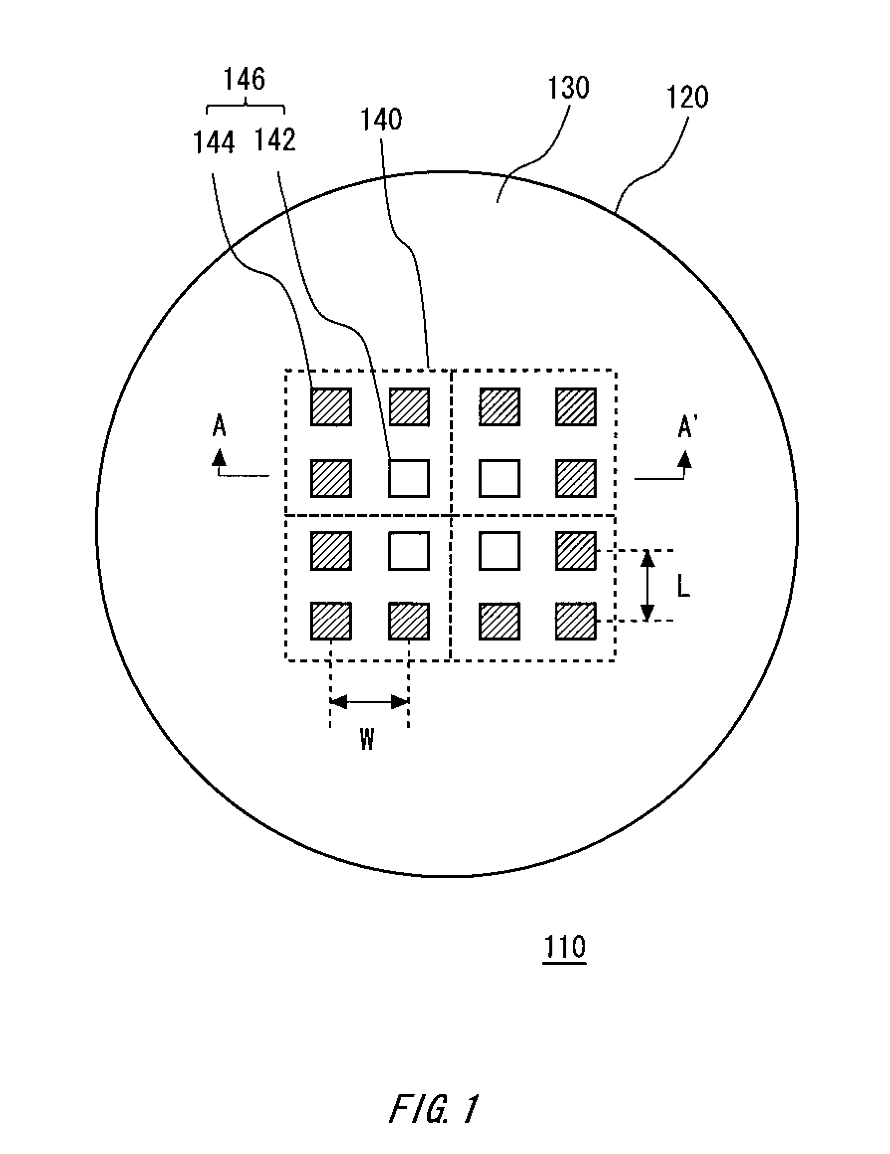
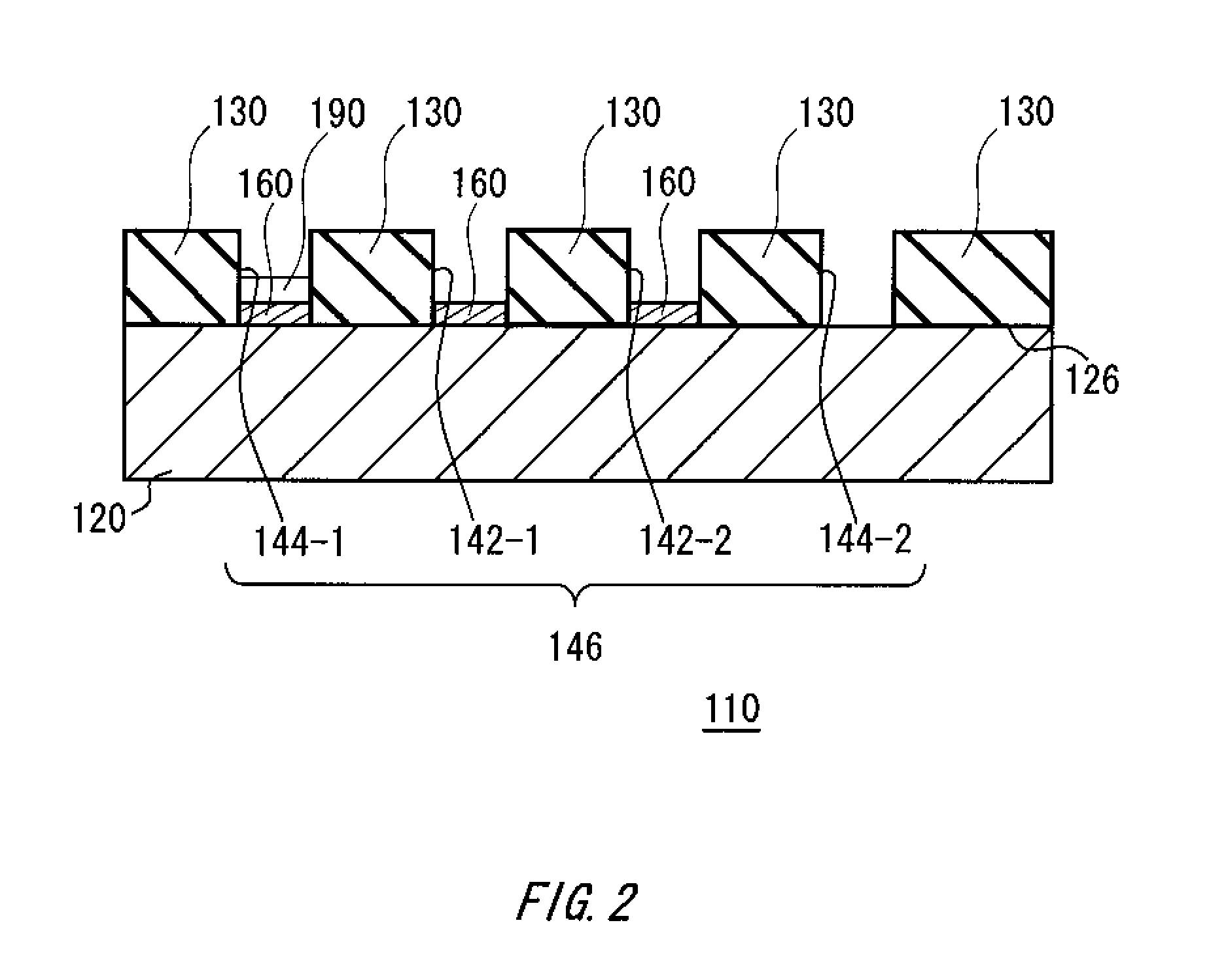
[0161]According to the procedures shown in FIG. 5 to FIG. 10, an electronic device 400 has been produced. A commercially-available SOI wafer was prepared as a base wafer 420. As an inhibition layer 430, a silicon oxide layer was prepared by CVD. The thickness of the silicon oxide layer was 1 μm. A plurality of openings were formed by photolithography. The plurality of openings were formed at constant intervals in both of the two directions orthogonal to each other, and have the same plane shape. The openings, each being a square whose a side has a length of 10 μm in the plan view, were arranged in a constant pitch of 30 μm therebetween. Since a side of the opening is 10 μm, the interval between two neighboring openings is 20 μm. The opening was designed to have a thickness of a seed crystal of 0.5 μm and a thickness of GaAs of 3 μm.

[0162]The seed crystal of Ge was formed inside the opening. The seed crystal of Ge was formed by CVD using halogen. The seed cry...

embodiment example no.2

Embodiment Example No. 2

[0166]According to the procedures shown in FIG. 5 to FIG. 8, crystal growth was conducted. A commercially-available Si wafer was prepared as a base wafer 420. As an inhibition layer 430, a silicon oxide layer was formed by a thermal oxidation method. The thickness of the silicon oxide layer was 1 μm. A plurality of openings were formed through the silicon oxide layer by photolithography. The plurality of openings having the same plane shape were formed at constant intervals. The openings, each being a square whose one side has a length of 10 μm in the plan view, were arranged in a constant pitch of 30 μm therebetween. In other words, the openings were formed at each distance of 30 μm. The Ge crystal was grown as a seed crystal to the thickness of 1 μm in the openings, and then was subjected to annealing. Thereafter, the GaAs crystal was grown.

[0167]A laser microscope was used to measure the crystal growth thickness in the center of each opening in the group o...

embodiment example no.3

Embodiment Example No. 3

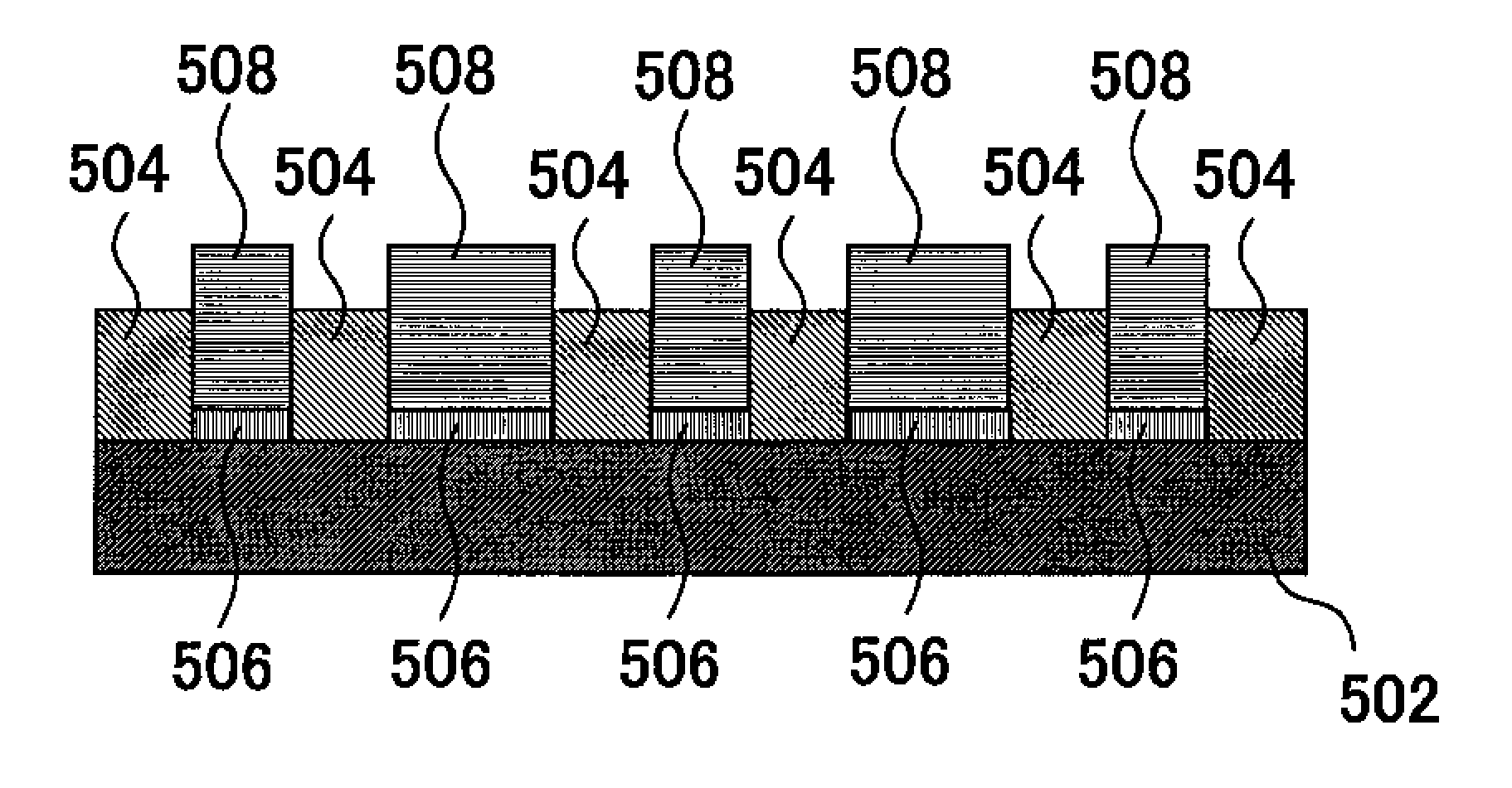
[0169]According to the procedures shown in FIG. 12A to FIG. 12D, an HBT was produced as an electronic device 500. A commercially-available Si wafer was prepared as a base wafer 502. As an inhibition layer 504, a silicon oxide layer was formed by a thermal oxidation method. The thickness of the silicon oxide layer was 1 μm. A plurality of isolated inhibition layers 504 were formed by photolithography. At the same time, openings A were provided through the inhibition layers 504. The plane shape of the inhibition layer 504 was a square having a side of 40 μm, and an opening A is provided in the center of the inhibition layer 504. The plane shape of the opening A was a square having a side of 20 μm. The inhibition layers 504 were formed at the constant interval of 50 μm pitch. Since a side of the inhibition layer 504 is 40 μm, a groove B was formed between two neighboring inhibition layers 504. The width of the groove B was 10 μm. The opening A was designed such ...


PUM


Abstract

The semiconductor wafer includes: a base wafer; and an inhibition layer that is disposed on the base wafer as one piece or to be separate portions from each other, and inhibits growth of a crystal of a compound semiconductor, where the inhibition layer has a plurality of first opening regions that have a plurality of openings penetrating the inhibition layer and leading to the base wafer, each of the plurality of first opening regions includes therein a plurality of first openings disposed in the same arrangement, some of the plurality of first openings are first element forming openings each provided with a first compound semiconductor on which an electronic element is to be formed, and the other of the plurality of first openings are first dummy openings in which no electronic element is to be formed.

Description

[0001]The contents of the following Japanese patent application and PCT patent application are incorporated herein by reference:[0002]JP2009-058730 filed on Mar. 11, 2009, and[0003]PCT / JP2010 / 001621 filed on Mar. 8, 2010.TECHNICAL FIELD[0004]The present invention relates to a semiconductor wafer, a method of producing a semiconductor wafer, an electronic device, and a method of producing an electronic device.BACKGROUND ART[0005]Recently, semiconductor devices using Group 3-5 compound semiconductors such as GaAs in an active region have been developed. For example, Patent Document 1 discloses a compound semiconductor epitaxial wafer in which crystal thin films of a buffer layer of AlGaAs and a channel layer of GaAs have been formed on a GaAs wafer.[0006]Patent Document 1: JP11-345812 ASUMMARY OF THE INVENTIONProblems to be Solved by the Invention [0007]When using a crystal thin film in an active region of a semiconductor device, it is required to form the crystal thin film having a u...

Claims


Application Information

Patent Timeline
IPC IPC(8): H01L29/165H01L21/20
CPCH01L21/0237H01L21/02381H01L21/02447H01L21/0245H01L21/02452H01L21/02463H01L29/772H01L21/02546H01L21/02642H01L29/107H01L29/73H01L29/7371H01L21/02538H01L21/20
Inventor TAKADA, TOMOYUKIHATA, MASAHIKOYAMANAKA, SADANORI
Owner SUMITOMO CHEM CO LTD
Why Eureka
Try Eureka