MEMS microphone and method for manufacturing same

a micro-electromagnetic system and microphone technology, applied in the direction of loudspeakers, liquid/solution decomposition chemical coatings, coatings, etc., can solve the problems of high manufacturing cost of condenser microphones, limited miniaturization of condenser microphones, and deformation or cracking of membranes, so as to reduce the number of manufacturing processes, prevent cracking, and reduce the residual stress of membranes and back plates

Inactive Publication Date: 2011-12-29
BSE CO LTD
View PDF6 Cites 21 Cited by
  • Summary
  • Abstract
  • Description
  • Claims
  • Application Information

AI Technical Summary

Benefits of technology

[0019]According to one or more embodiments of the present invention, since a membrane and a back plate are formed by electroless plating, it is not required to perform a separate high temperature heating process in order to inject metallic ions into polysilicon, thereby reducing the number of manufacturing processes of a micro electro mechanical systems (MEMS) microphone.
[0020]Since the membrane and the back plate are formed at a low temperature (about 90° C.) by electroless plating, a MEMS chip and an application specific integrated (ASIC) chip may be formed as a single chip. In addition, the MEMS microphone may be manufactured by using a unified semiconductor manufacturing method.
[0021]Since the MEMS microphone is manufactured at a low temperature, even though thermal expansion coefficients of the membrane and the back plate are different, a residual stress generated in the membrane and the back plate may be reduced. In addition, a contact region between the silicon substrate and the membrane and the back plate may be prevented from cracking.
[0022]Since the membrane and the back plate are formed by electroless plating, the thicknesses of the membrane and the back plate may be easily adjusted, thereby stabilizing acoustic features and increasing acoustic sensitivity.
[0023]Since an air gap is formed by etching the silicon substrate followed by forming the membrane and the back plate, the air gap may be correctly and simply formed. Furthermore, the height of the MEMS microphone may be reduced, and the membrane and the back plate may be stably fixed to the silicon substrate.
[0024]Since a sacrificial layer is formed on an air-gap forming portion of the silicon substrate, it is not required to form or etch a separate layer in order to form the sacrificial layer, thereby reducing the number of manufacturing processes.

Problems solved by technology

Thus, the manufacturing costs of the condenser microphone are high, and there is a limit in miniaturizing the condenser microphone.
As the residual stress acts on the membrane, the membrane may be deformed or may crack.
Furthermore, since the residual stress acts on the membrane, it may be difficult for the membrane to correctly vibrate according to a sound, and thus, it may be difficult to correctly convert a sound into an electrical signal.
In addition, since an oxidizing speed of silicon of the porous silicon structure may be changed according to a voltage condition, the back volume may not be uniformly etched.
When a surface of the back volume is not be uniformly etched, a distance between the diaphragm and the back plate is not constant, and thus, it may be difficult to correctly convert a sound into an electrical signal.
In this case, since the manufacturing method includes manufacturing an application specific integrated (ASIC) chip including a circuit formed by patterning a metallic material and then manufacturing a MEMS chip, it is difficult to manufacture the MEMS chip and the ASIC chip as a single chip.
This is because when the ASIC chip is exposed to a high temperature during manufacture of the MEMS ship, the ASIC chip may be melted or damaged.
Furthermore, since it is difficult to form the MEMS chip and the AISIC chip as a single chip, the MEMS chip and the ASIC chip may be separately manufactured, thereby increasing the number of manufacturing processes and manufacturing costs.
Accordingly, there is a limit in manufacturing a miniaturized microphone.

Method used


Image

  • MEMS microphone and method for manufacturing same
  • MEMS microphone and method for manufacturing same
  • MEMS microphone and method for manufacturing same

Examples


Embodiment Construction

[0044]Hereinafter, a micro electro mechanical systems (MEMS) microphone will be described with regard to exemplary embodiments of the invention with reference to the attached drawings.

[0045]A MEMS microphone according to an embodiment of the present invention will be described below.

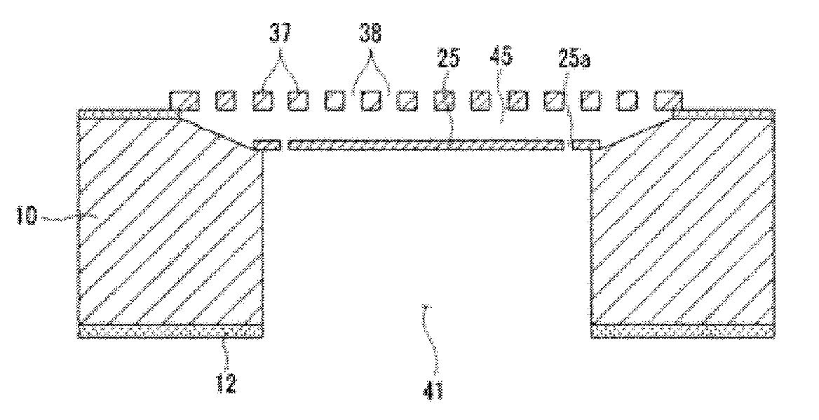
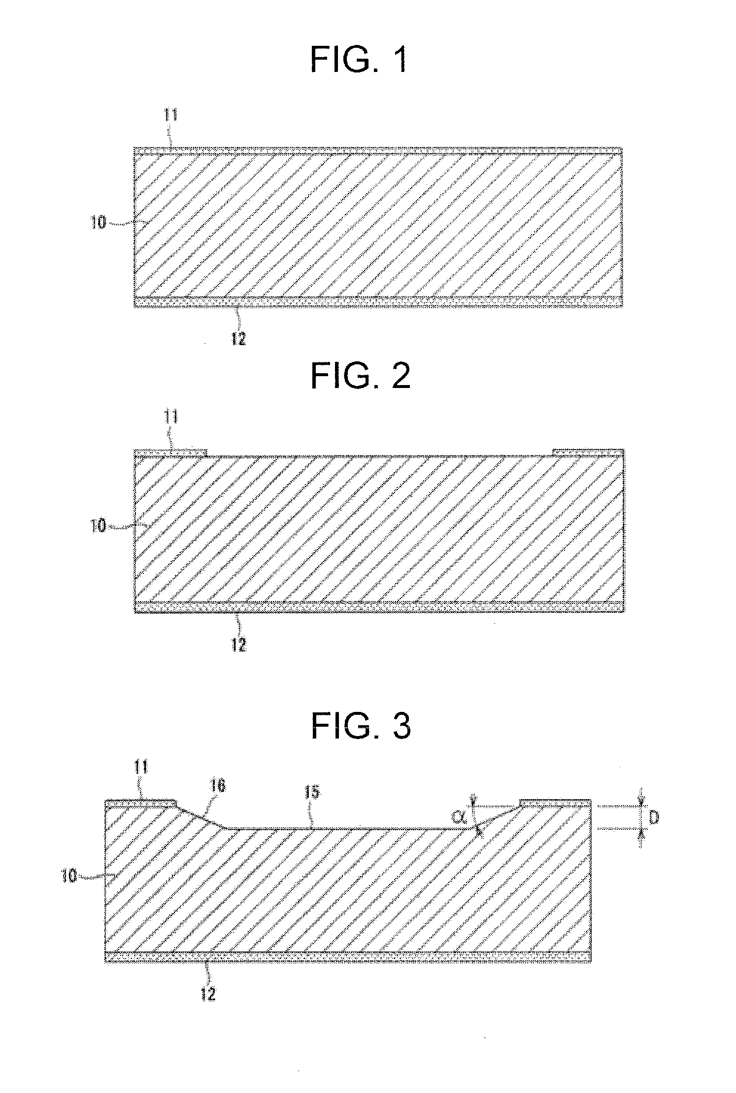
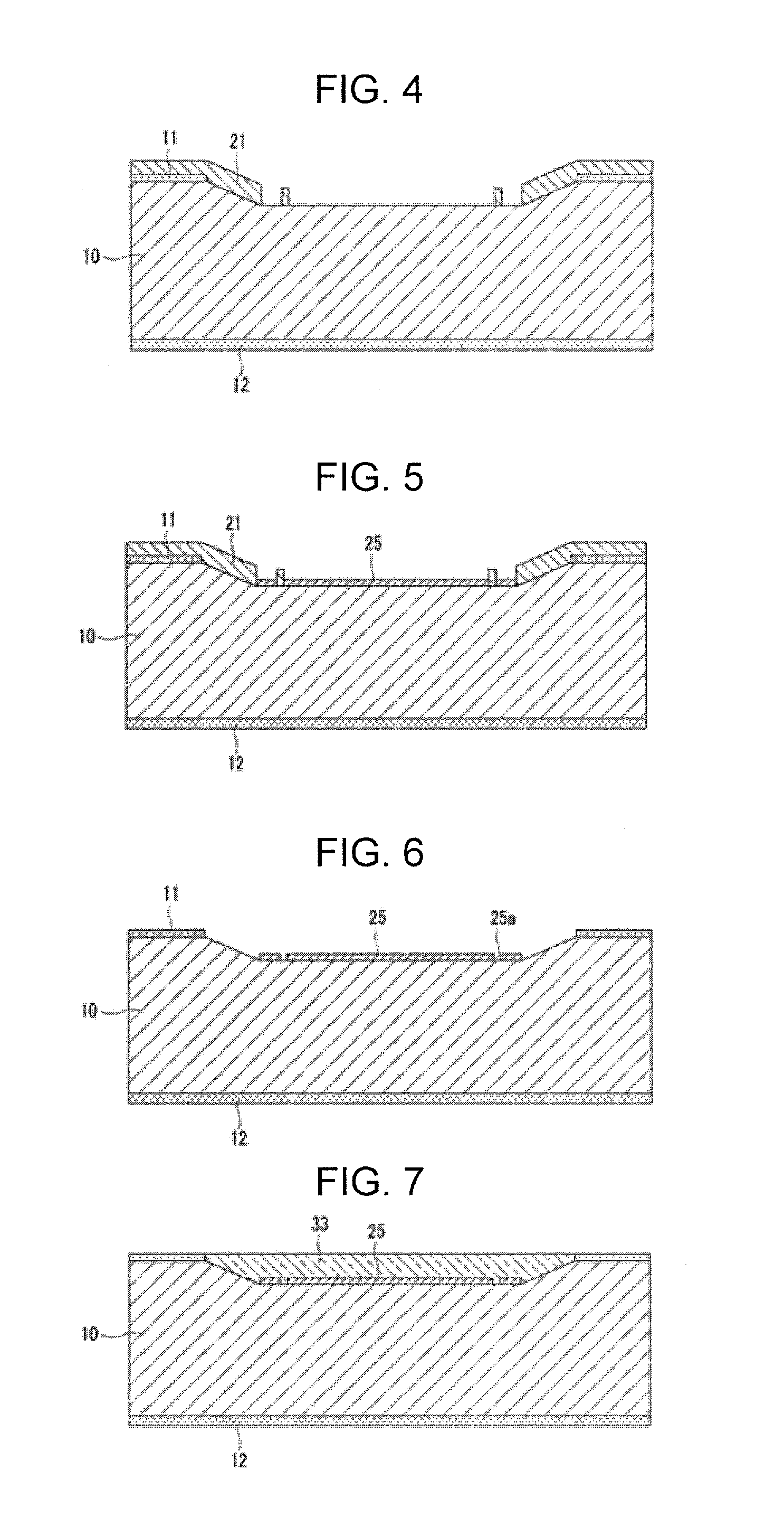
[0046]FIGS. 1 through 3 are cross-sectional views for explaining a process of forming an air-gap forming portion 15 on a silicon substrate 10 in a MEMS microphone according to an embodiment of the present invention.

[0047]Referring to FIGS. 1 and 2, the MEMS microphone according to the present embodiment includes the silicon substrate 10. Insulating protective layers 11 and 12 are formed by depositing silicon nitride (Si3N4) or silicon oxide (SiO2) on two sides of the silicon substrate 10, respectively (refer to FIGS. 1 and 2). In this case, the insulating protective layers 11 and 12 are formed by depositing Si3N4 on a surface of the silicon substrate 10 by using a low pressure chemical vapor deposition (...


PUM

PropertyMeasurementUnit
temperatureaaaaaaaaaa
inclination angleaaaaaaaaaa

Abstract

A micro electro mechanical systems (MEMS) microphone, and a method of manufacturing the MEMS microphone having an interval between a membrane and a back plate, the interval being correctly adjusted by forming the membrane and the back plate after an air-gap forming portion on a silicon substrate. Since the membrane and/or the back plate are/is formed by electroless plating, a sacrificial layer is easily planarized, and a residual stress is easily removed or controlled. The MEMS microphone includes a silicon substrate in which a back chamber is formed and on which an air-gap forming portion is formed above the chamber by etching the silicon substrate to a predetermined depth above the chamber; a membrane formed on the air-gap forming portion of the silicon substrate or the silicon substrate; and a back plate that is formed on the air-gap forming portion or the silicon substrate so as to be spaced apart from the membrane, wherein an air gap is formed between the membrane and the back plate.

Description

TECHNICAL FIELD[0001]One or more aspects of the present invention relate to micro electro mechanical systems (MEMS) microphones and methods of manufacturing the same.BACKGROUND ART[0002]A microphone is a device for converting a voice into an electrical signal. The microphone may be used in various mobile communication devices such as mobile terminals, and various communication devices such as earphones or hearing aids. The microphone needs to have excellent electronic / audible performance, reliability, and operability.[0003]Examples of the microphone include a condenser microphone and a micro electro mechanical systems (MEMS) microphone.[0004]The condenser microphone is manufactured by respectively manufacturing a diaphragm, a back plate, a signal-processing printed circuit board (PCB), and the like, and then assembling these components in a case. In order to manufacture the condenser microphone, the PCB is separately manufactured. Thus, the manufacturing costs of the condenser micro...

Claims


Application Information

Patent Timeline
Patent Type & Authority Applications(United States)
IPC IPC(8): H01L29/84H01L21/306H01L21/20
CPCB81B2201/0257H04R19/04B81C1/00158B81B2203/0127C23C18/16H04R31/006H04R2201/003
Inventor KIM, YONG-KOOKSONG, CHUNG-DAM
Owner BSE CO LTD
Why Eureka
Try Eureka