
Patsnap Eureka
For R&D, Patsnap Eureka makes reading and utilizing patents & technical documents easy.
Patsnap Eureka AIR
Designed for self-driven R&D workflows. Generate viable solutions, solve complex R&D challenges, empower your innovation with AI.

Patsnap Eureka Materials
Designed for material experts only. Revolutionize your material R&D, from search, analyze, to developing new materials.

TechResearch
Generate reliable direction feasibility study reports for your R&D in just a few steps.

TechSeek
Discover and master advanced knowledge NOW. Basics, ideas, possibilities, all at once.

TechMind
As an expert in R&D Theories, TechMind can generates customized viable solutions instantly.

TechRisk
Analyze your overall solution with one click, know your potential R&D risks in advance.

TechMonitor
Get weekly tech updates, stay abreast of the latest tech innovations and key insights.
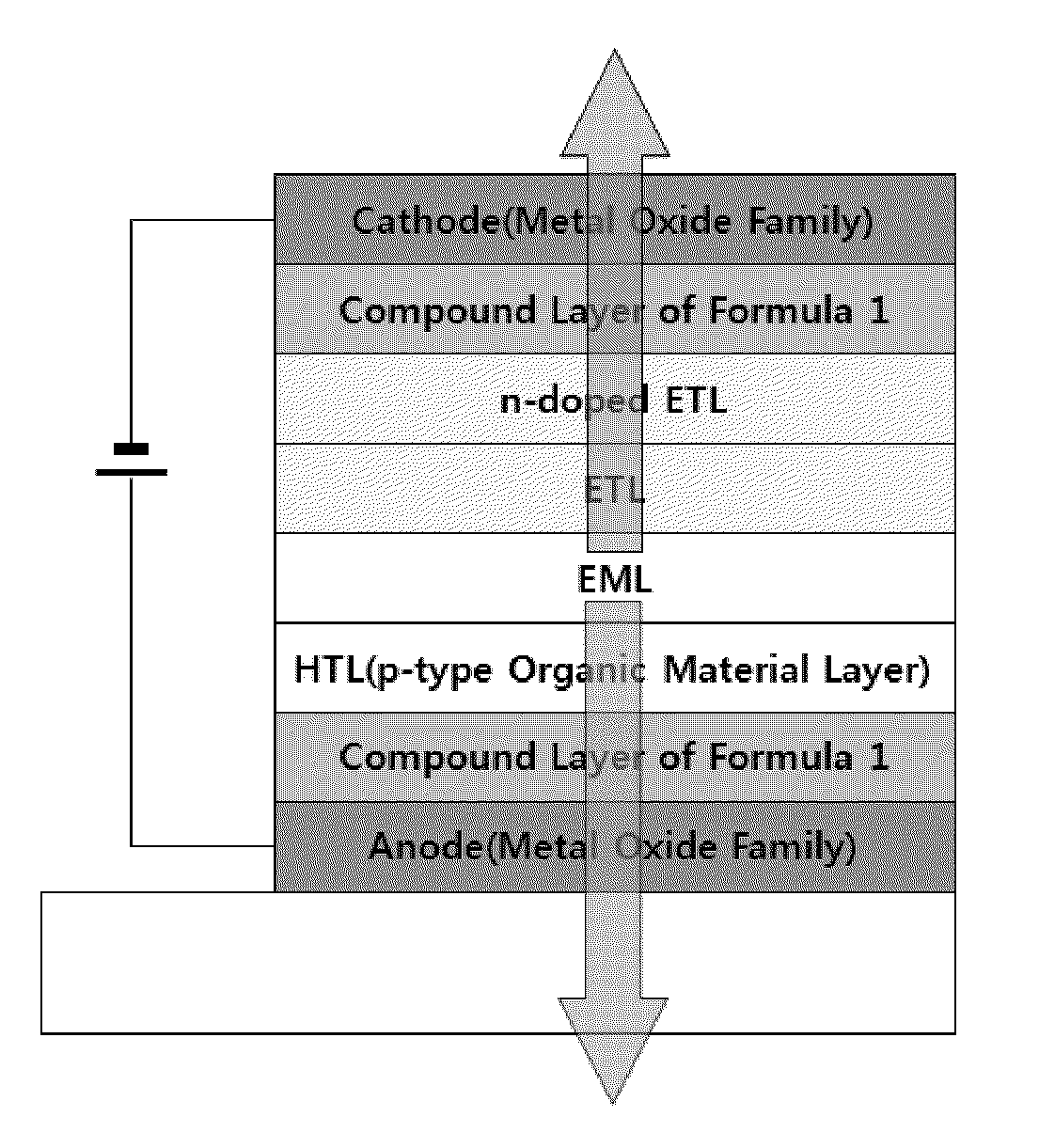
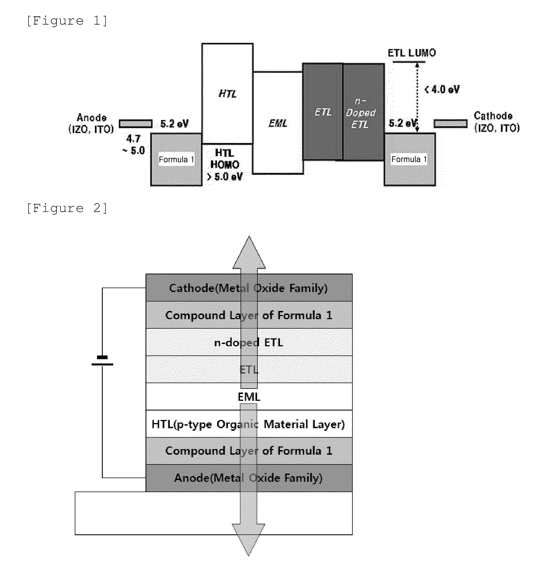
Organic light-emitting device, and method for manufacturing same
a light-emitting device and organic technology, applied in the direction of organic semiconductor devices, thermoelectric devices, organic chemistry, etc., can solve the problems of affecting the work efficiency the inability to use resistive heating evaporation methods, and the loss of electroconductivity and visible ray transmittance, so as to prevent the damage of the organic material layer and achieve high work function
- Summary
- Abstract
- Description
- Claims
- Application Information
AI Technical Summary
Benefits of technology
Problems solved by technology
Method used
Image

Examples
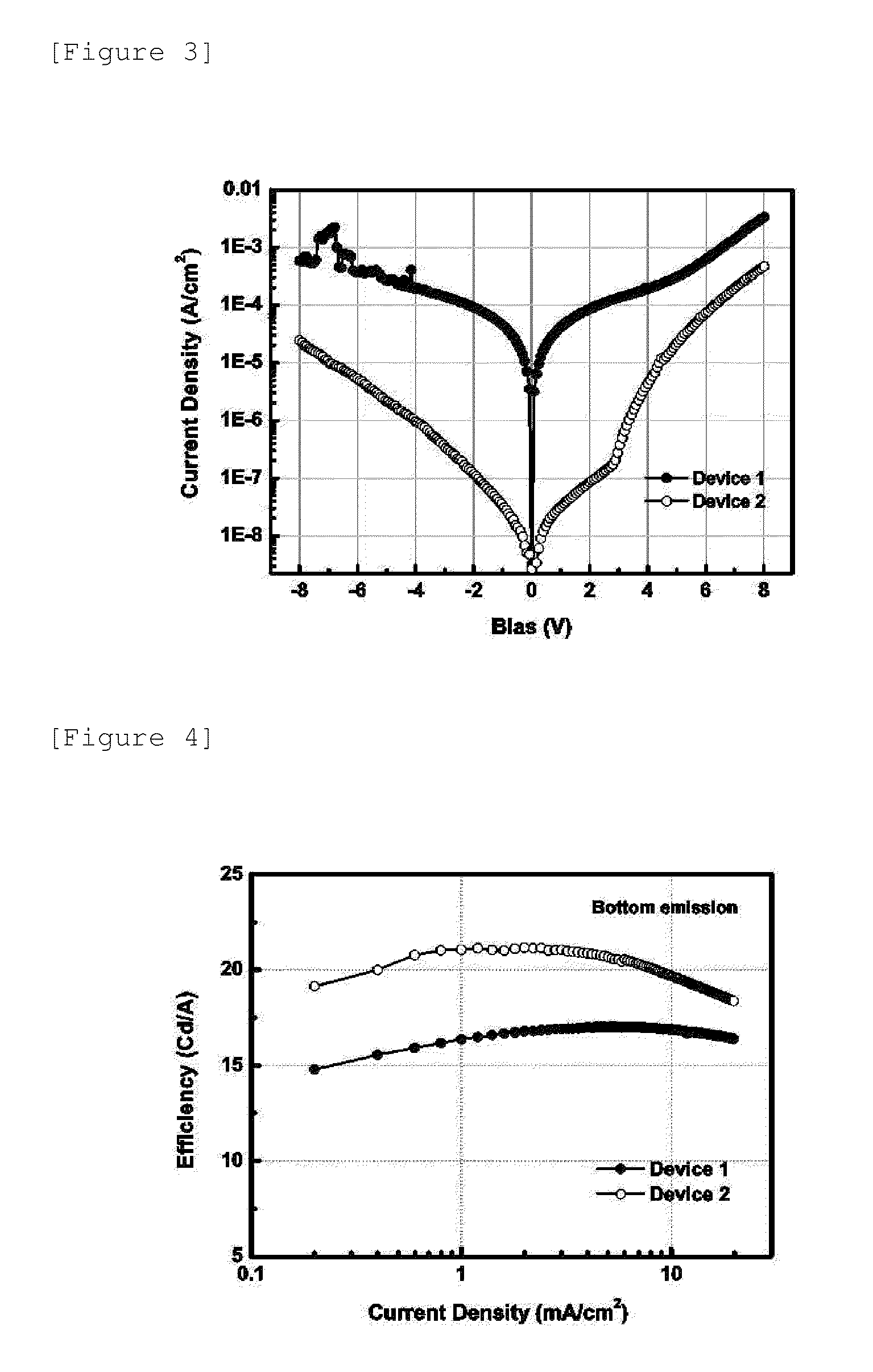
example 1
[0063]The transparent anode (first electrode) having the thickness of 1000 Å was formed on the substrate by the sputtering method using IZO, the hole injection layer having the thickness of 500 Å was formed thereon by vacuum depositing HAT by heat, and the hole transport layer having the thickness of 400 Å was formed thereon by vacuum depositing NPB of the following Formula.
[0064]In addition, Ir(ppy)3 of the following Formula was doped into CBP of the following Formula in the amount of 10 wt %, and the light emitting layer having the thickness of 300 Å was configured by the doped organic layer.
[0065]In addition, BAlq that was the hole blocking layer material of the following Formula was formed thereon in a thickness of 50 Å.
[0066]The electron transport material of the following Formula was formed thereon in a thickness of 150 Å, and the electron transport layer having the thickness of 50 Å doped by doping Ca to the electron transport material of the following Formula in the amount o...
example 2
[0087]The transparent anode (first electrode) having the thickness of 1000 Å was formed on the substrate by the sputtering method using IZO, the hole injection layer having the thickness of 500 Å was formed thereon by vacuum depositing HAT by heat, and the hole transport layer having the thickness of 400 Å was formed thereon by vacuum depositing NPB of the above Formula.
[0088]In addition, Ir(ppy)3 of the above Formula was doped into CBP of the above Formula in the amount of 10 wt % to configure the light emitting layer having the thickness of 300 Å, and BAlq that was the hole blocking layer material was formed thereon in a thickness of 50 Å.
[0089]The electron transport material used in Example 1 was formed thereon in a thickness of 150 Å, and the electron transport layer having the thickness of 50 Å doped by doping Ca to the electron transport material used in Example 1 in the amount of 10 wt % was formed thereon. LiF that was the metal salt was deposited in the thickness of 15 Å th...
example 3
[0094]The transparent anode (first electrode) having the thickness of 1000 Å was formed on the substrate by the sputtering method using IZO, and Ag was deposited thereon in the thickness of 200 Å. The hole injection layer having the thickness of 500 Å was formed on deposited Ag by vacuum depositing HAT by heat, and the hole transport layer having the thickness of 400 Å was formed thereon by vacuum depositing NPB of the above Formula.
[0095]In addition, Ir(ppy)3 of the above Formula was doped into CBP of the above Formula in the amount of 10 wt % to configure the light emitting layer having the thickness of 300 Å, and BAlq that was the hole blocking layer material was formed thereon in a thickness of 50 Å.
[0096]The electron transport material used in Example 1 was formed thereon in a thickness of 150 Å, and the electron transport layer having the thickness of 50 Å doped by doping Ca to the electron transport material used in Example 1 in the amount of 10 wt % was formed thereon. LiF t...
PUM
 Abstract
Description
Claims
Application Information
 - R&D Engineer
- R&D Manager
- IP Professional
- Industry Leading Data Capabilities
- Powerful AI technology
- Patent DNA Extraction
Browse by: Latest US Patents, China's latest patents, Technical Efficacy Thesaurus, Application Domain, Technology Topic, Popular Technical Reports.
© 2024 PatSnap. All rights reserved.Legal|Privacy policy|Modern Slavery Act Transparency Statement|Sitemap|About US| Contact US: help@patsnap.com