Semiconductor device and manufacturing method thereof

a semiconductor device and manufacturing method technology, applied in semiconductor devices, semiconductor/solid-state device details, electrical devices, etc., can solve the problems of increasing the diameter, increasing the influence of warpage, and difficulty in aligning the mask, so as to prevent the occurrence of warpage in the wafer, enhance the accuracy of patterning, and ensure the effect of high-quality semiconductor devices

Inactive Publication Date: 2012-01-12
PANASONIC CORP
View PDF1 Cites 18 Cited by
  • Summary
  • Abstract
  • Description
  • Claims
  • Application Information

AI Technical Summary

Benefits of technology

[0033]As has been described in detail, in the semiconductor device of the present invention, occurrence of warpage in a wafer is prevented, and accuracy of patterning is enhanced. Therefore, a highly reliable semiconductor device can be provided with high accuracy.
[0034]Since forming trenches in the respective scribe regions is realized in the same step of production of trench gates, manufacturing cost can be curtailed.
[0035]A geometry of trenches can be made stable, and occurrence of variations in electrical characteristic can be prevented. Reliability of the semiconductor device can be enhanced.

Problems solved by technology

An increase in the diameter of the wafer leads to an increase in the influence of warpage.
Difficulty is eventually encountered in aligning a mask when element regions are formed by use of; for instance, photolithography, and when a photoresist is exposed to light.
Another problem is that a fracture or cracking occurs during conveyance of a wafer.
Moreover, when the wafer is separated into chips after cutting trenches have been formed by the dicing saw and when an adhesive tape affixed to the wafer is extended to cut, stress imposed on the wafer becomes greater, which in turn raises a problem of occurrence of chipping.
These problems lead to a decrease in production yield of a semiconductor device, which in turn incurs an increase in manufacturing cost.
Therefore, a problem of warpage of a wafer is now a serious problem.

Method used


Image

  • Semiconductor device and manufacturing method thereof
  • Semiconductor device and manufacturing method thereof
  • Semiconductor device and manufacturing method thereof

Examples


first embodiment

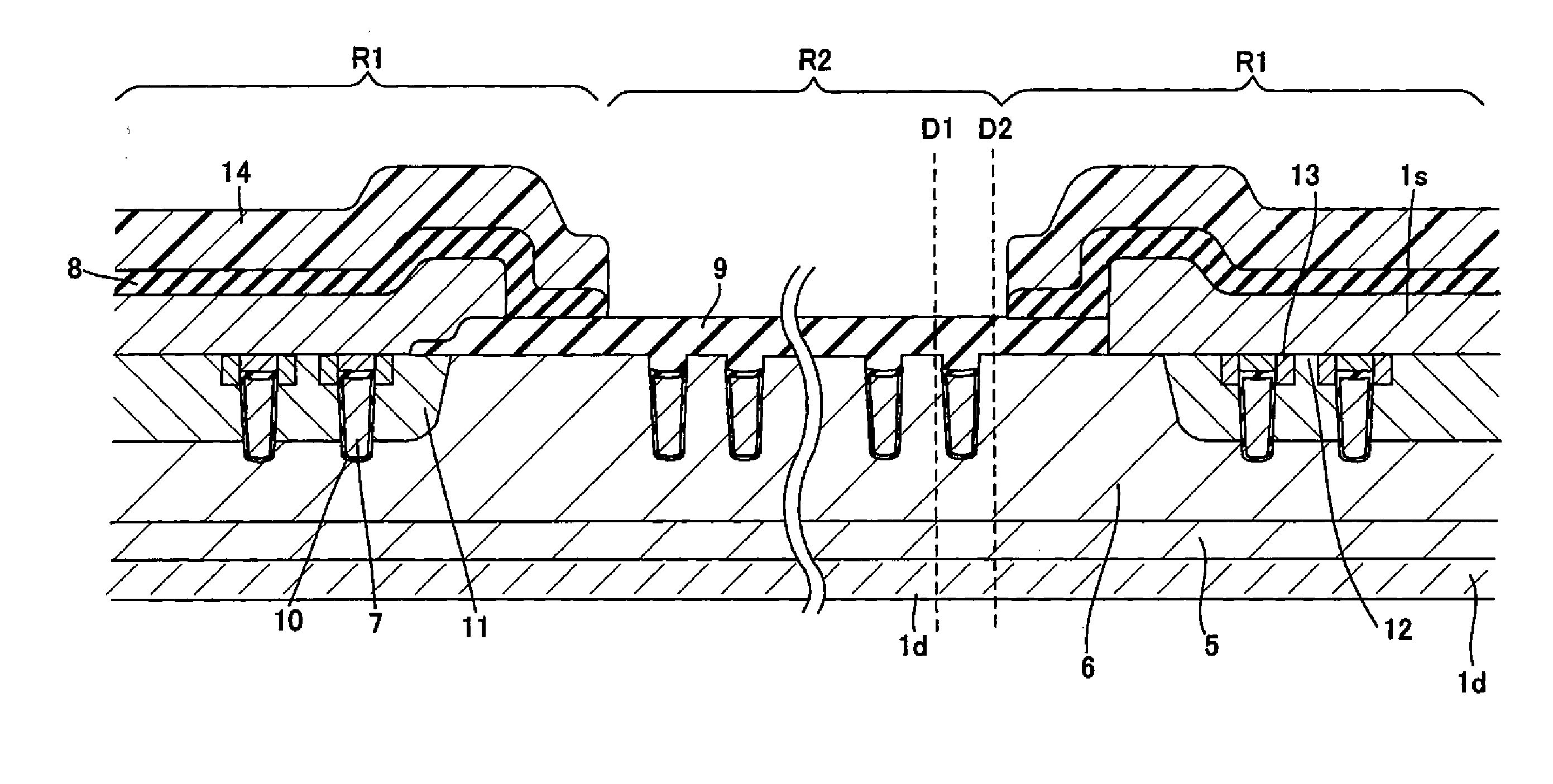
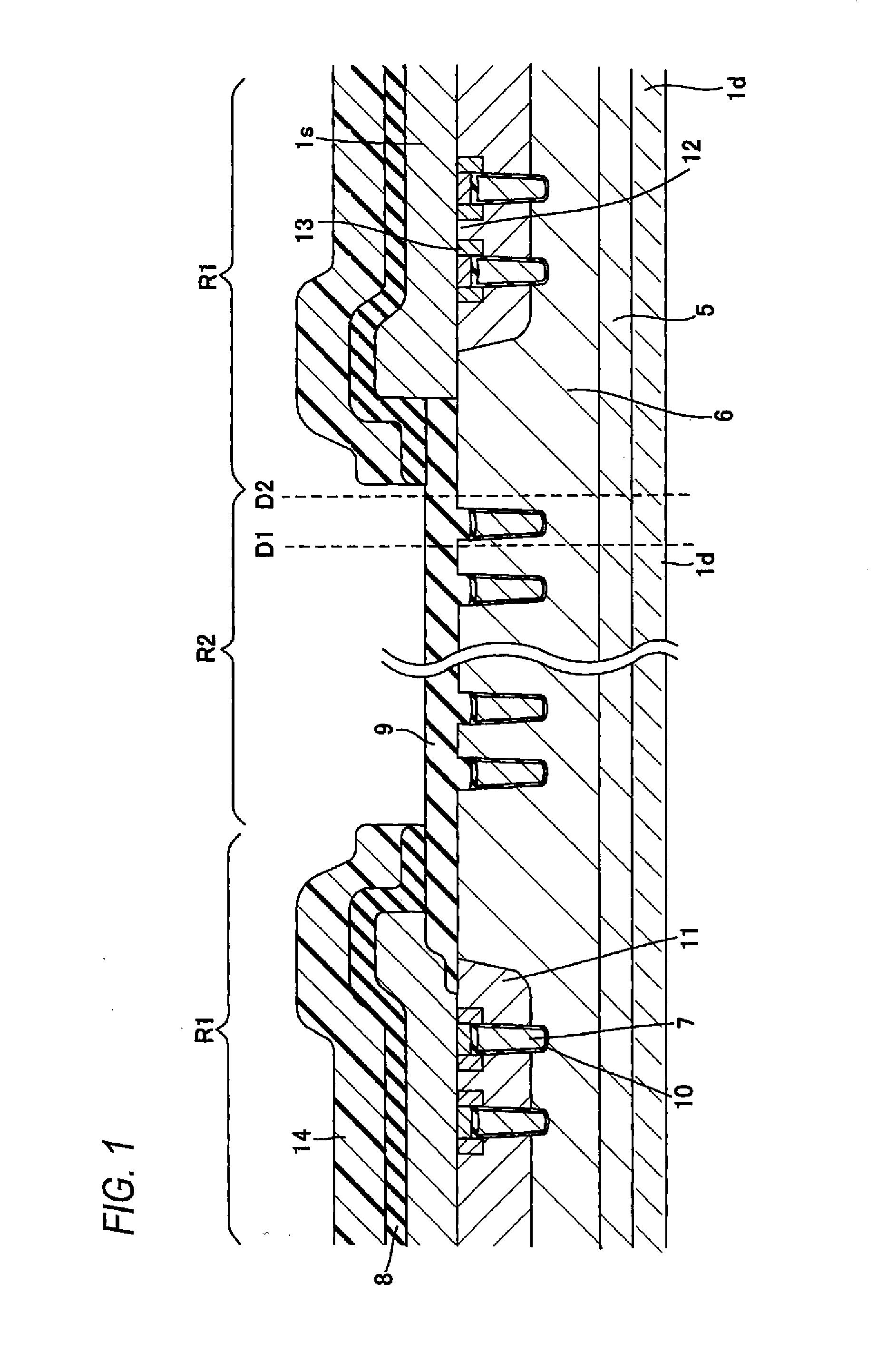
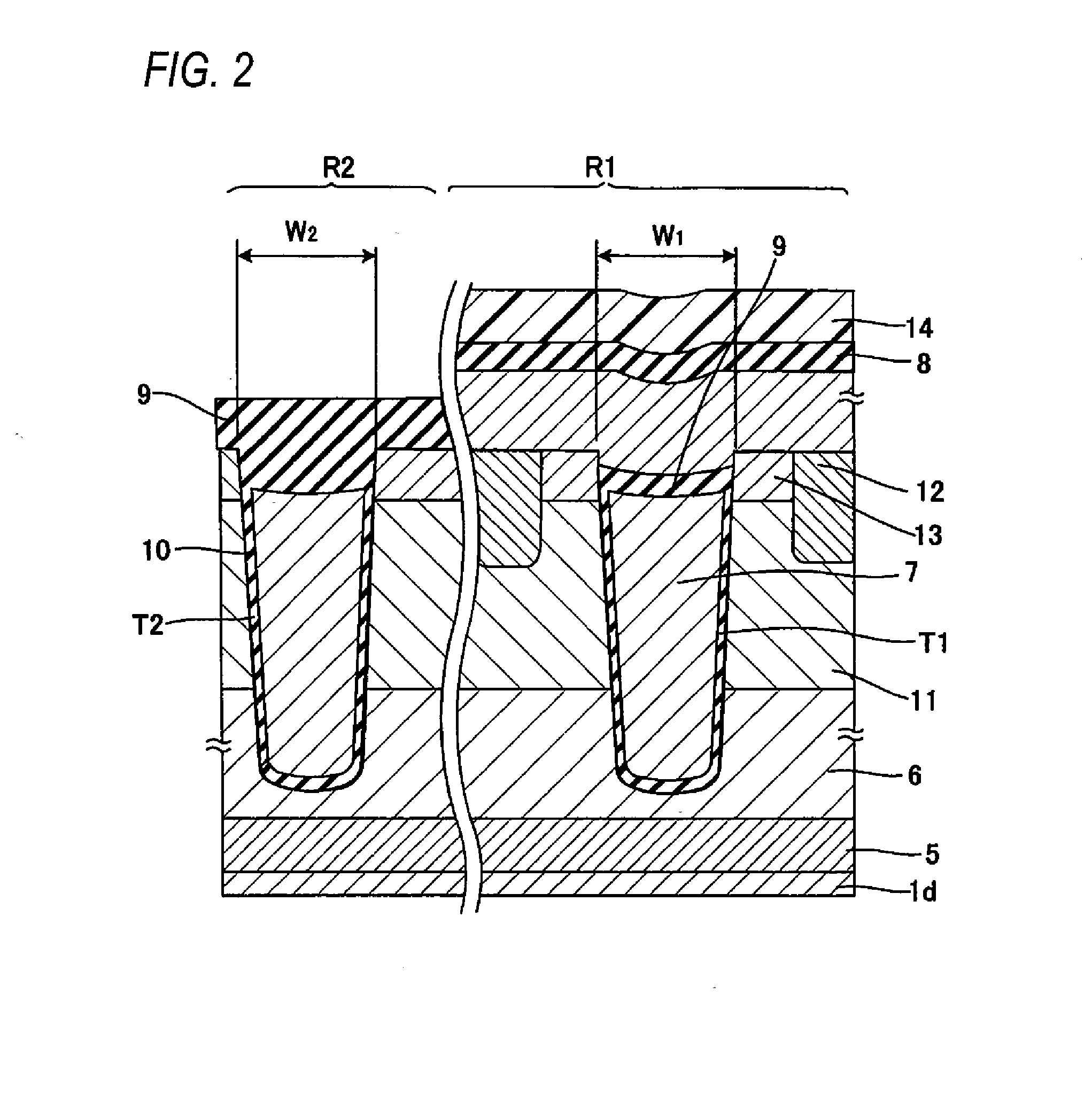
[0045]FIG. 1 is an explanatory view showing an edge portion of a trench MOSFET of a first embodiment of the present invention. FIG. 2 is an enlarged view of the principal portion. FIGS. 3 and 4 are overall views of the trench MOSFET. FIG. 3 is a top view, and FIG. 4 is a cross sectional view taken along line A-A shown in FIG. 3. FIGS. 5(a) to (d) are views showing a step for manufacturing the trench MOSFET of the first embodiment. FIGS. 1 and 2 are equivalent to a cross section taken along line B-B shown in FIG. 3.

[0046]As shown in FIGS. 1 through 4, the trench MOSFET of the present embodiment is a semiconductor device having a trench gate in an element region formed in a semiconductor substrate. The MOSFET is characterized in that second trenches T2 having the same depth as that of first trenches T1 making up the trench gate are provided along a marginal area of the semiconductor substrate. A width W1 of each of the first trenches T1 is assumed to be equal to a width W2 of each of ...

second embodiment

[0065]A second embodiment of the present invention is now described.

[0066]In the second embodiment, the direction of the second trenches T2 in the scribe regions R2 of the first embodiment is changed as shown in FIG. 7, and the second trenches T2 are formed so as to become parallel to the first trenches T1. Even in this case, the first trenches T1 and the second trenches T2 are simultaneously formed.

[0067]By means of the configuration, since all of the first trenches T1 and the second trenches T2 run in the same direction, stable patterning becomes possible. A broken line designates one chip unit.

third embodiment

[0068]A third embodiment of the present invention is now described.

[0069]In the third embodiment, as shown in FIG. 8, the second trenches T2 are formed in the scribe regions R2 so as to assume the width W2 that is greater than the width W1 of the first trenches T1. The semiconductor device is analogous to that described in connection with the preceding embodiments in terms of the other configuration.

[0070]The configuration makes formation of a mask pattern easy and enables performance of stable patterning operation.

[0071]In the embodiment, the second trenches T2 are filled with polycrystalline silicon, but the trenches T2 may also be filled with an insulating material, like polyimide.

[0072]The present embodiment has provided descriptions about the trench MOSFET. However, the present embodiment is not limited to the MOSFET but also applicable to another element having a trench structure, such as an insulated gate bipolar transistor (IGBT), a trench capacitor, and DRAM.


PUM


Abstract

A semiconductor device having trench gates in element regions R1 formed in a semiconductor substrate. Second trenches T2 having the same depth as that of first trenches T1 making up the trench gates are provided along a marginal area of the semiconductor substrate.

Description

TECHNICAL FIELD[0001]The present invention relates to a semiconductor device and manufacturing method thereof and, more particularly, to lessening of warpage of a wafer in a semiconductor device, like an insulated gate transistor having a trench structure.BACKGROUND ART[0002]With a reduction in power consumption, greater sophistication, and a speedup of electronic devices, including a portable phone, a growing demand recently exists for a reduction in power consumption and a speedup of a semiconductor device accommodated in the electronic devices. To meet the demand, transistors exhibiting smaller on-resistance are generally required for transistors used in load switches of electronic devices, DC-DC converters, and the like. One proposed method for reducing on-resistance of a transistor is to miniaturize individual devices to thereby increase density of transistors to be placed per unit area. Specifically, a density of transistors in a vertical MOSFET having gate electrodes formed i...

Claims


Application Information

Patent Timeline
Patent Type & Authority Applications(United States)
IPC IPC(8): H01L27/088H01L21/8234
CPCH01L23/562H01L29/0657H01L29/0696H01L29/407H01L29/4238H01L29/66734H01L2924/0002H01L29/7811H01L29/7813H01L2924/00
Inventor OOTA, TOMONARI
Owner PANASONIC CORP
Why Eureka
Try Eureka