Metal Oxide Semiconductor Thin Film Transistors

Inactive Publication Date: 2012-01-19
SHARP KK
View PDF4 Cites 28 Cited by
  • Summary
  • Abstract
  • Description
  • Claims
  • Application Information

AI Technical Summary

Benefits of technology

[0008]Described herein is a method for modifying an oxide semiconductor film composition with the desired result of reducing costly elements, improving performance, and creating a larger processing space window. The oxide semiconductor films mentioned below incorporate a variety of elements into the films that help control carrier concentrations.

Problems solved by technology

Unfortunately, InGaZnOx films are expensive to fabricate due to the high cost of the In and Ga used in the films.

Method used


Image

  • Metal Oxide Semiconductor Thin Film Transistors
  • Metal Oxide Semiconductor Thin Film Transistors
  • Metal Oxide Semiconductor Thin Film Transistors

Examples


Embodiment Construction

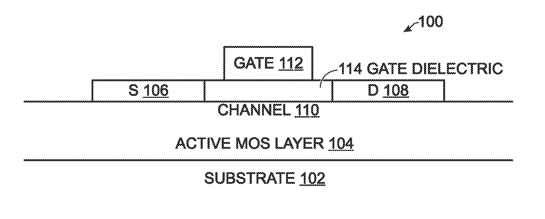
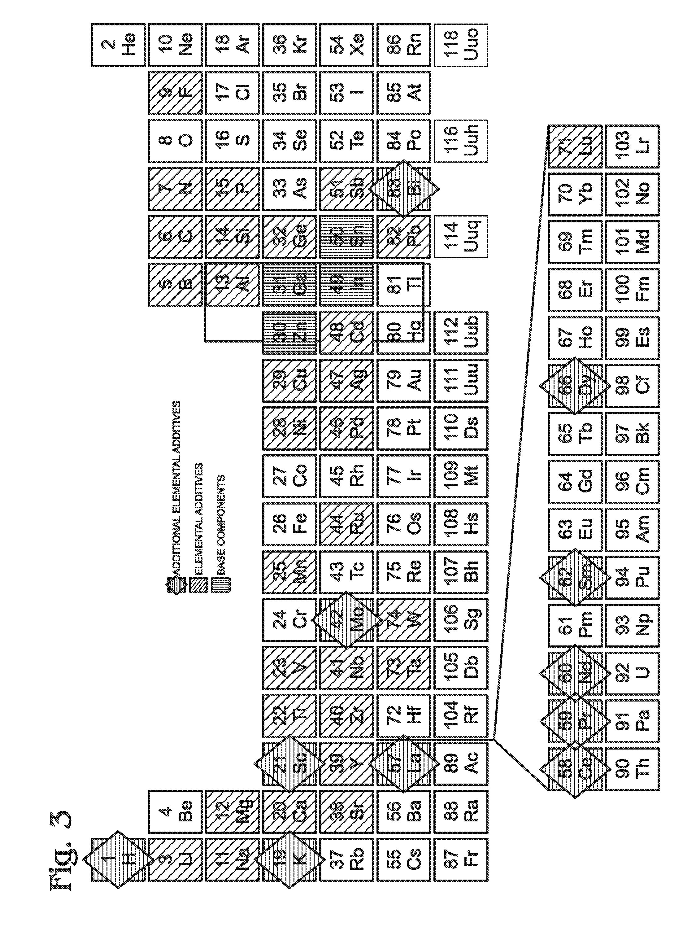
[0015]FIG. 1 is a partial cross-sectional view of a top gate thin film transistor (TFT). The top gate TFT 100 comprises a substrate 102 made from a semiconductor material, such as silicon, or transparent material, such as glass, quartz, or plastic. An active metal oxide semiconductor (MOS) layer 104 overlies the substrate 102. The active MOS layer 104 is a material such as ZnOx, InOx, GaOx, SnOx, or combinations of the above-mentioned materials. For example, the active MOS layer 104 may be ZnSnOx, InGaZnOx, ZnInOx, or InGaOx. The active MOS layer 104 also includes a primary dopant of H, K, Sc, La, Mo, Bi, Ce, Pr, Nd, Sm, Dy, or combinations of the above-mentioned dopants. In one aspect, the primary dopant is H, Mo, or a combination of H and Mo. In another aspect, the active MOS layer 104 is InGaZnOx and the primary dopant is Mo.

[0016]Source / drain (S / D) regions 106 and 108, respectively, are formed in contact with the active MOS layer 104. In one aspect, S / D regions 106 / 108 may be me...


PUM


Abstract

A top gate and bottom gate thin film transistor (TFT) are provided with an associated fabrication method. The TFT is fabricated from a substrate, and an active metal oxide semiconductor (MOS) layer overlying the substrate. Source / drain (S / D) regions are formed in contact with the active MOS layer. A channel region is interposed between the S / D regions. The TFT includes a gate electrode, and a gate dielectric interposed between the channel region and the gate electrode. The active MOS layer may be ZnOx, InOx, GaOx, SnOx, or combinations of the above-mentioned materials. The active MOS layer also includes a primary dopant such as H, K, Sc, La, Mo, Bi, Ce, Pr, Nd, Sm, Dy, or combinations of the above-mentioned dopants. The active MOS layer may also include a secondary dopant.

Description

BACKGROUND OF THE INVENTION[0001]1. Field of the Invention[0002]This invention generally relates to integrated circuit (IC) and display backplane fabrication and, more particularly, to metal oxide semiconductor (MOS) thin film transistors made from doped of ZnOx, InOx, GaOx, and SnOx materials.[0003]2. Description of the Related Art[0004]Currently, a variety of materials are being used for oxide semiconductor based thin film transistors with metal oxide semiconductors (MOS) as the active semiconducting materials (see for example, “Transparent Electronics”, J. Wager, D. Keszler, R. Presley, Springer, 2007). At this time, the primary materials of choice include ZnO and InGaZnOx. Very good electrical performance can be obtained for thin film transistors (TFT) devices fabricated with these materials. For example, InGaZnOx TFTs can be used to drive pixels for electrophoretic, liquid crystal display (LCD), and organic light emitting diode (OLED) displays.[0005]It should also be noted that...

Claims


Application Information

Patent Timeline
IPC IPC(8): H01L29/786H01L21/34H01L21/336H01L29/12
CPCH01L21/02554H01L21/02565H01L29/66969H01L29/7869H01L21/02581
Inventor HERMAN, GREGORYMAA, JER-SHENPUNTAMBEKAR, KANANVOUTSAS, APOSTOLOS T.
Owner SHARP KK
Why Eureka
Try Eureka