Semiconductor device

Active Publication Date: 2012-01-19
SEMICON ENERGY LAB CO LTD
View PDF17 Cites 31 Cited by
  • Summary
  • Abstract
  • Description
  • Claims
  • Application Information

AI Technical Summary

Benefits of technology

[0010]In view of the foregoing problems, an object of one embodiment of the present invention is to provide a semiconductor device with a novel structure in which stored data can be retained even w

Problems solved by technology

Moreover, in the case of a transistor formed using a highly purified oxide semiconductor, the l

Method used


Image

  • Semiconductor device
  • Semiconductor device
  • Semiconductor device

Examples


Example

Embodiment 1

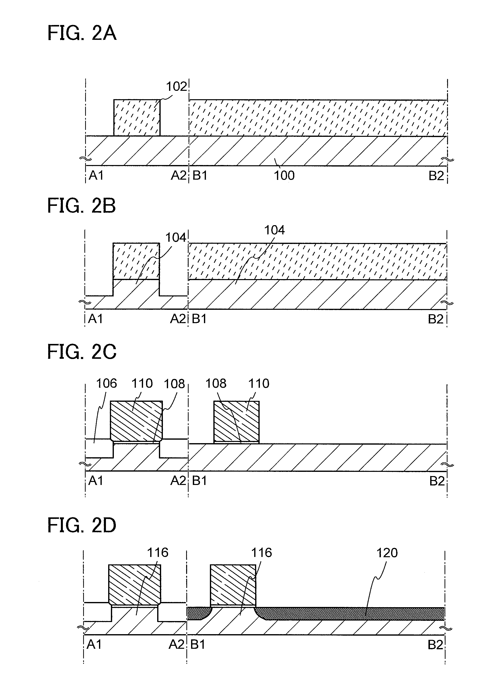
[0040]In this embodiment, a structure and a manufacturing method of a semiconductor device according to one embodiment of the present invention will be described with reference to FIGS. 1A and 1B, FIGS. 2A to 2D, FIGS. 3A to 3D, FIGS. 4A to 4D, FIGS. 5A and 5B, FIGS. 6A and 6B, and FIGS. 7A-1, 7A-2, and 7B.

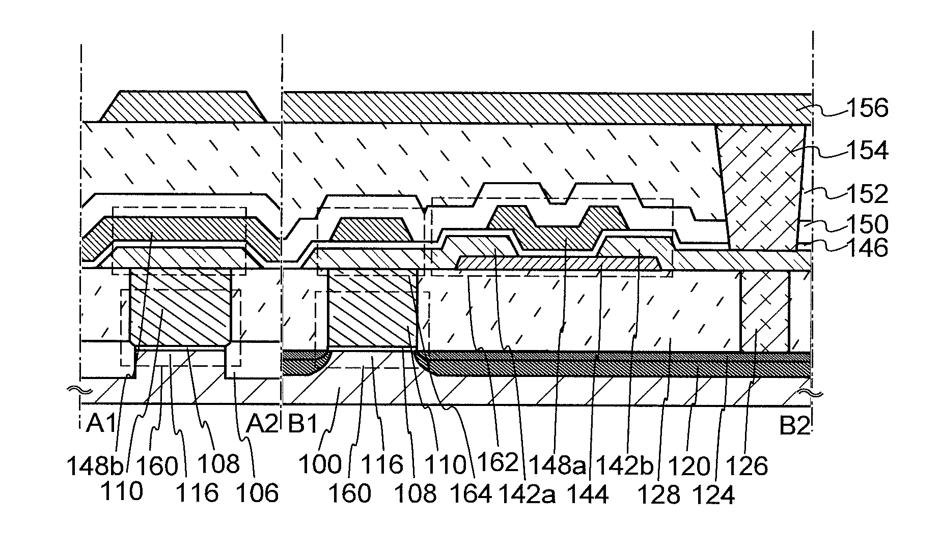
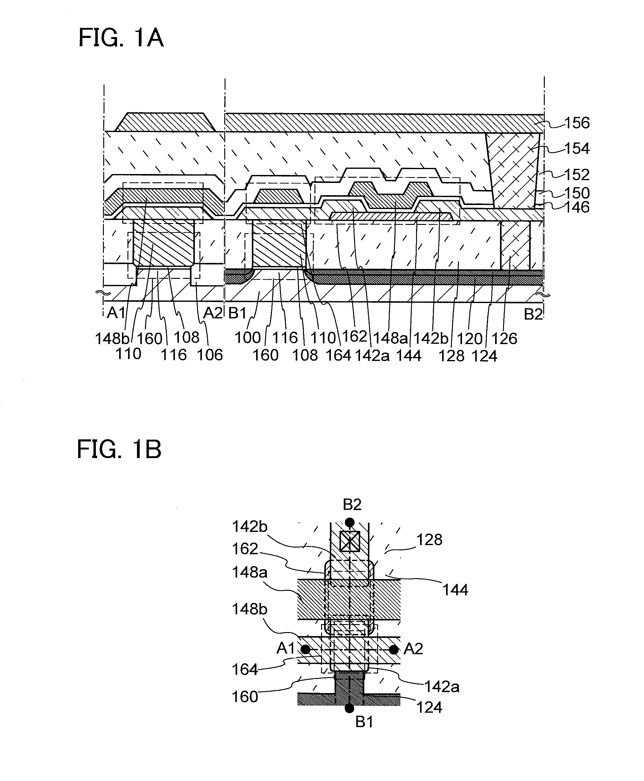
[0041]FIGS. 1A and 1B illustrate an example of a structure of a semiconductor device. FIG. 1A is a cross-sectional view of the semiconductor device. FIG. 1B is a plan view of the semiconductor device. In FIG. 1A, the cross section A1-A2 is perpendicular to the channel length direction of a transistor, and the cross section B1-B2 is parallel to the channel length direction of the transistor. The semiconductor device illustrated in

[0042]FIGS. 1A and 1B includes a transistor 160 including a first semiconductor material in a lower portion, and a transistor 162 including a second semiconductor material in an upper portion. FIGS. 1A and 1B show that the semiconductor device ...

Example

Embodiment 2

[0178]In this embodiment, an application example of a semiconductor device according to one embodiment of the present invention will be described with reference to FIGS. 8A to 8C and FIGS. 9A to 9C. Here, an example of a storage device will be described. Note that in circuit diagrams, “OS” is sometimes written beside a transistor in order to indicate that the transistor includes an oxide semiconductor.

[0179]FIGS. 8A to 8C are circuit diagrams of semiconductor devices each of which can be used as a storage device and includes a plurality of semiconductor devices (hereinafter also referred to as memory cells) illustrated in FIG. 7A-1. Each of FIGS. 8A and 8B is a circuit diagram of a NAND semiconductor device in which memory cells are connected in series. FIG. 8C is a circuit diagram of a NOR semiconductor device in which memory cells are connected in parallel.

[0180]The semiconductor device in FIG. 8A includes a source line SL, a bit line BL, a first signal line S1, m seco...

Example

Embodiment 3

[0211]In this embodiment, application of the semiconductor device described in any of the above embodiments to an electronic device will be described with reference to FIGS. 10A to 10F. In this embodiment, examples of the electronic device to which the above semiconductor device is applied are a computer, a mobile phone (also referred to as a cell phone or a mobile phone device), a personal digital assistant (including a portable game machine and an audio reproducing device), a camera such as a digital camera and a digital video camera, electronic paper, and a television device (also referred to as a television or a television receiver).

[0212]FIG. 10A illustrates a laptop personal computer that includes a housing 701, a housing 702, a display portion 703, a keyboard 704, and the like. The semiconductor device described in the above embodiment is provided in at least one of the housing 701 and the housing 702. Thus, it is possible to realize a laptop personal computer in ...


PUM


Abstract

A semiconductor device with a novel structure in which stored data can be retained even when power is not supplied, and does not have a limitation on the number of write cycles. The semiconductor device includes a memory cell including a first transistor, a second transistor, and an insulating layer placed between a source region or a drain region of the first transistor and a channel formation region of the second transistor. The first transistor and the second transistor are provided to at least partly overlap with each other. The insulating layer and a gate insulating layer of the second transistor satisfy the following formula: (ta/tb)×(εrarb)<0.1, where ta represents the thickness of the gate insulating layer, tb represents the thickness of the insulating layer, εra represents the dielectric constant of the gate insulating layer, and εrb represents the dielectric constant of the insulating layer.

Description

TECHNICAL FIELD[0001]One embodiment of the present invention relates to a semiconductor device using a semiconductor element and a method for manufacturing the semiconductor device.BACKGROUND ART[0002]Storage devices using semiconductor elements are broadly classified into two categories: a volatile device that loses stored data when power supply stops, and a non-volatile device that retains stored data even when power is not supplied.[0003]A typical example of a volatile storage device is a DRAM (dynamic random access memory). A DRAM stores data in such a manner that a transistor included in a storage element is selected and electric charge is stored in a capacitor.[0004]When data is read from a DRAM, electric charge in a capacitor is lost on the above principle; thus, another write operation is necessary every time data is read out. Moreover, since a transistor included in a storage element has a leakage current between a source and a drain in an off state (i.e., an off-state curr...

Claims


Application Information

Patent Timeline
IPC IPC(8): H01L27/088
CPCG11C16/0433G11C16/26H01L27/11517H01L27/088H01L27/1211H01L27/1225H01L27/1156H10B41/00H10B41/70
Inventor YAMAZAKI, SHUNPEIKATO, KIYOSHINAGATSUKA, SHUHEI
Owner SEMICON ENERGY LAB CO LTD
Why Eureka
Try Eureka