Constant voltage regulator

a constant voltage regulator and constant voltage technology, applied in the direction of electric variable regulation, process and machine control, instruments, etc., can solve the problems of discharge circuit , overshoot protection provided by the comparator , runaway or other failure of the load circuit supplied therewith

Active Publication Date: 2012-01-19
NISSHINBO MICRO DEVICES INC
View PDF5 Cites 40 Cited by
  • Summary
  • Abstract
  • Description
  • Claims
  • Application Information

AI Technical Summary

Problems solved by technology

If not corrected, voltage overshoot above the maximum allowable limit of the output voltage can result in runaway or other failures of the load circuit supplied therewith.
One drawback of this method is that overshoot protection provided by the comparator 440 and the discharge circuit 450 does not effectively work, where the comparator 440 exhibits a certain amount of offset voltage that causes a delay in responding to voltage overshoot.
Moreover, the voltage regulator 401 requires a substantial amount of current consumed by the comparator 440 to obtain prompt comparator response for effective overshoot protection, which, however, makes it difficult to implement the voltage regulator 401 in an integrated circuit (IC) that consumes low current during operation.
Such method has a drawback in that it requires a large value or size of capacitor and resistors forming the overshoot protection circuit to properly protect against voltage overshoot, where the power supply voltage as well as the output voltage rise upon power-on with a time constant larger than that which is determined by the driver transistor's ON-resistance and load current, and the capacitance connected to the output terminal.
Due to such size requirement for the capacitor and resistors, which makes it difficult to implement the voltage regulator on a single IC, this method remains impractical or otherwise unduly expensive to practice.
As is the case with the overshoot protection circuit depicted above, such method has a drawback in that it requires a large value or size of capacitor and resistor forming the soft start circuit to properly protect against voltage overshoot, where the power supply voltage rises upon power-on with a time constant larger than that which is determined by the driver transistor's ON-resistance and load current, and the capacitance connected to the output terminal.
Due to such size requirement for the capacitor and resistor, which makes it difficult to implement the voltage regulator on a single IC, this method remains impractical or otherwise unduly expensive to practice.
Such method has a drawback in that it cannot effectively protect against voltage overshoot in case the drain current flowing through the driver transistor remains extremely low, for example, where the power supply voltage rises upon power-on with a time constant larger than that which is determined by the driver transistor's-ON resistance and load current, and the capacitance connected to the output terminal.
Either of such methods using a filter-based overshoot detector has a drawback in that it requires a large value or size of capacitor and resistor forming the RC filter to properly protect against voltage overshoot, where the power supply voltage rises upon power-on with a time constant larger than that which is determined by the driver transistor's ON-resistance and load current, and the capacitance connected to the output terminal.
Due to such size requirement for the capacitor and resistor, which makes it difficult to implement the voltage regulator on a single IC, this method remains impractical or otherwise unduly expensive to practice.

Method used


Image

  • Constant voltage regulator
  • Constant voltage regulator
  • Constant voltage regulator

Examples


first embodiment

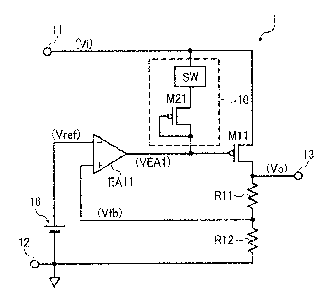
[0056]FIG. 8 is a circuit diagram schematically illustrating a constant voltage regulator 1 according to this patent specification.

[0057]As shown in FIG. 8, the constant voltage regulator 1 comprises a series regulator for power supply control in electronic devices, such as personal computers, cellular phones, and the like, which converts an input voltage Vi supplied between an input terminal 11 and a ground terminal 12 to a regulated, constant output voltage Vo for output to an output terminal 13 connected to load circuitry that operates with a rated voltage of, for example, 3.3 volts.

[0058]The voltage regulator 1 includes a driver transistor M11, being a p-channel metal-oxide semiconductor (PMOS) device, having a source terminal thereof connected to the input terminal 11 and a drain terminal thereof connected to the output terminal 13; a pair of voltage divider resistors R11 and R12 connected in series between the output terminal 13 and the ground terminal 12 to form a feedback ge...

second embodiment

[0078]FIG. 12 is a circuit diagram schematically illustrating the constant voltage regulator 1 according to this patent specification.

[0079]As shown in FIG. 12, the overall configuration of the present embodiment is similar to that depicted in FIG. 8, except that the differential gain controller 10 includes a pair of first and second, diode-connected PMOS transistors M24 and M25, instead of a single diode-connected transistor M21, each connected in series with the switch SW.

[0080]Specifically, in the present embodiment, the first differential amplifier EA11 has a substantially symmetrical configuration including a differential pair of n-channel metal-oxide semiconductor (NMOS) transistors M12 and M13, the former having its gate terminal connected to the reference voltage generator 16, and the latter having its gate terminal connected to the feedback node between the voltage divider resistors R11 and R12; a current-mirror active load formed of a pair of PMOS transistors M14 and M15, ...

third embodiment

[0091]FIG. 14 is a circuit diagram schematically illustrating the constant voltage regulator 1 according to this patent specification.

[0092]As shown in FIG. 14, the overall configuration of the present embodiment is similar to that depicted in FIG. 8, except that the differential gain controller 10 derives a current for conduction to the gate of the driver transistor M11 from the output terminal 13 instead of the input terminal 11 of the voltage regulator 1.

[0093]Specifically, in the present embodiment, the switch SW is disposed between the output terminal 13 and the output of the first differential amplifier EA11. The diode-connected transistor M21 has a source terminal thereof connectable to the output terminal 13 via the switch SW, and gate and drain terminals thereof connected together to the output of the differential amplifier EA11.

[0094]In such a configuration, the gain controller 10 controls the gain G of the first differential amplifier EA11 in a manner similar to that depi...


PUM


Abstract

A voltage regulator includes a driver transistor, a feedback voltage generator, a reference voltage generator, a first differential amplifier, and a differential gain controller. The driver transistor is connected between input and output terminals to conduct a current therethrough according to a control signal applied to a gate terminal thereof. The feedback voltage generator is connected to the output terminal to generate a feedback voltage. The reference voltage generator generates a reference voltage. The first differential amplifier has an output thereof connected to the gate terminal of the driver transistor, and a pair of differential inputs thereof connected to the feedback voltage generator and the reference voltage generator, respectively, to generate the control signal at the output thereof. The differential gain controller is connected to the output of the first differential amplifier to control the differential gain according to a difference between the input and output voltages.

Description

BACKGROUND OF THE INVENTION[0001]1. Technical Field[0002]The present invention relates to a constant voltage regulator, and more particularly, to a constant voltage regulator for power supply circuitry in electronic devices, such as personal computers and cellular phones, implementable in a low-current consumption integrated circuit (IC), which converts an input voltage input to an input terminal thereof into a regulated, output voltage output to an output terminal thereof.[0003]2. Description of the Background Art[0004]Voltage regulators are employed in power supply circuitry of various electronic devices, such as personal computers and cellular phones, which converts an input voltage input to an input terminal thereof into a regulated, output voltage for output to load circuitry, such as a microcontroller or other electronic components.[0005]FIG. 1 is a circuit diagram schematically illustrating a configuration of a known constant voltage regulator 101.[0006]As shown in FIG. 1, th...

Claims


Application Information

Patent Timeline
Patent Type & Authority Applications(United States)
IPC IPC(8): G05F1/10
CPCG05F1/565
Inventor MORINO, KOICHI
Owner NISSHINBO MICRO DEVICES INC
Why Eureka
Try Eureka