Granular channel width for power optimization

a power optimization and channel width technology, applied in the direction of cad circuit design, program control, instruments, etc., can solve the problems of continuous power waste, difficult to fully switch off transistors, and static power consumption in conventional digital cmos processes, etc., to achieve the effect of optimizing performance and power

Active Publication Date: 2012-01-26
BELL SEMICON LLC
View PDF1 Cites 86 Cited by
  • Summary
  • Abstract
  • Description
  • Claims
  • Application Information

AI Technical Summary

Benefits of technology

[0007]The objects, features and advantages of the present invention may include providing a granular channel width for power optimization that may (i) allow a foundry independent approach for using granular channel widths to optimize performance and power, (ii) allow the design of a cell with a maximum driver size, a minimum driver size, and a number of intermediate driver sizes, while generally remaining within Design Rule Check (DRC) parameters, (iii) allow the design of a cell that may be characterized for power and performance at the minimum driver size, maximum driver size, and the intermediate driver sizes, (iv) create a lookup table so that power and performance may be estimated with any final driver size, (v) provide a tool that affords a large granularity of cells across the power and performance spectrum, (vi) remove large step functions in power and performance that prevent Leakage In Place Optimization (LIPO) tools from doing an optimal job, (vii) note information for use in redefining the cell with the appropriate diffusion (OD) area and device width, after the LIPO tool estimates the correct driver size for the best power / performance tradeoff, (viii) allow device width corrections to be done at any point in the design flow, (ix) introduce the ability to target dynamic power reduction via positive slack recovery late in the design flow with zero to minimal design impact and / or (x) introduce the ability to target static or dynamic power recovery as appropriate for the application.

Problems solved by technology

Static power consumption in conventional digital CMOS processes is usually the result of transistors that do not act as perfect switches.
The transistors are difficult to switch off fully.
The leakage current results in a continuous waste of power.
Transistors with a higher Vt will have worse performance (i.e., the transistor is slower to switch on and has less drive current when on).

Method used


Image

  • Granular channel width for power optimization
  • Granular channel width for power optimization
  • Granular channel width for power optimization

Examples


Embodiment Construction

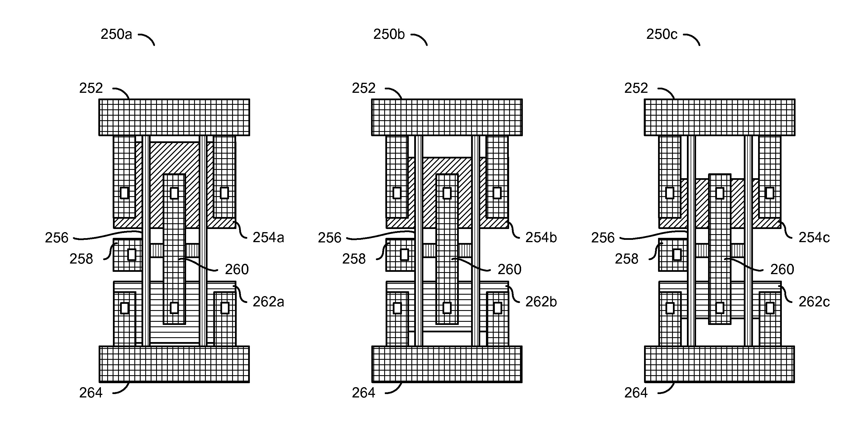
[0015]Static power consumption may be mitigated by using different transistor channel lengths. For the libraries with different channel lengths to be footprint compatible, the libraries may all be designed to the dimensions of the largest channel length. Libraries may be created that offer several (e.g., three or more) channel length options and / or several (e.g., three or more) Vt options that may have the same footprint to permit power reduction and precise performance / power optimization.

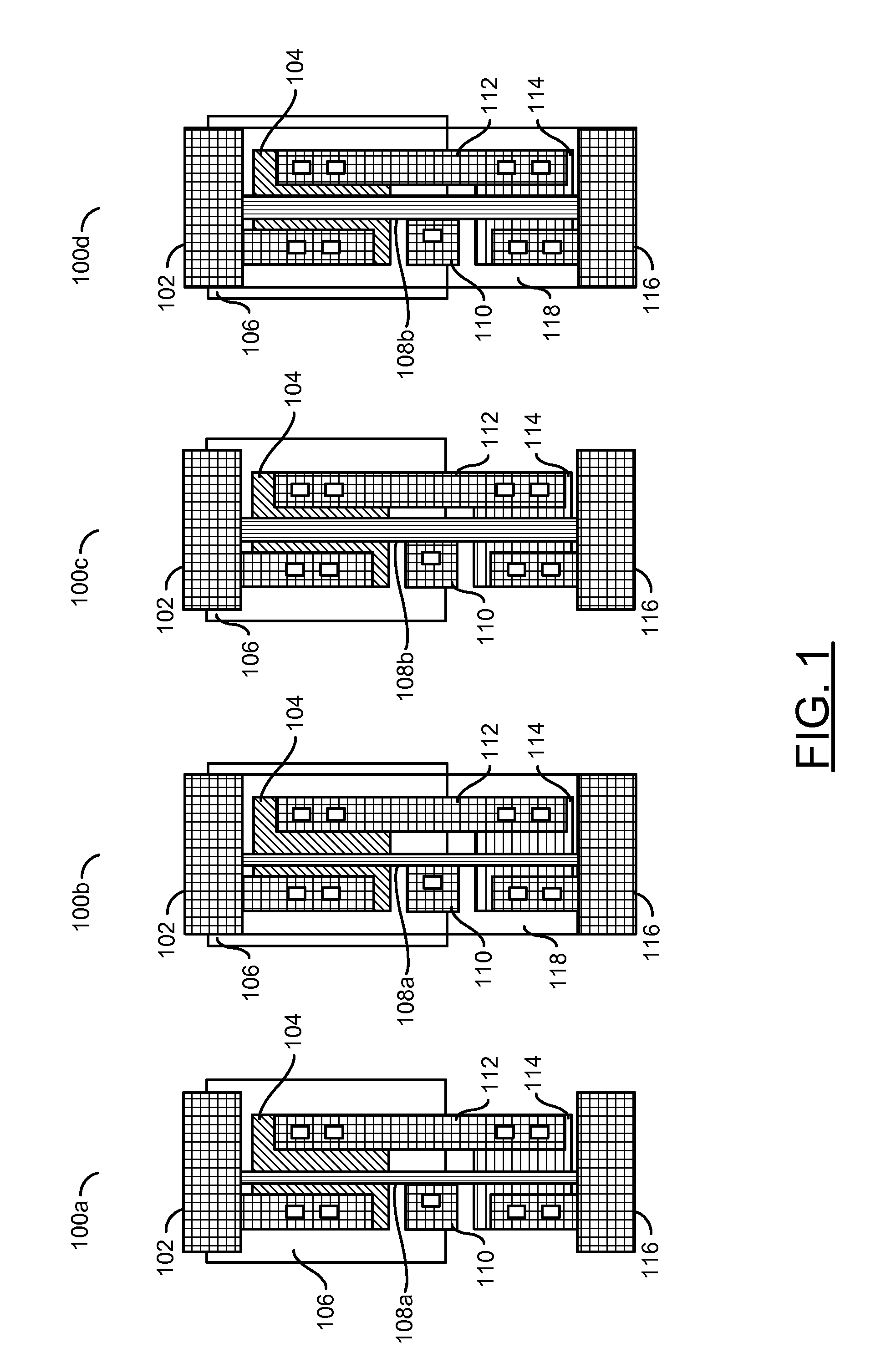
[0016]Referring to FIG. 1, a diagram illustrating a variety of cells 100a-100d with Vt and channel length variations is shown. Each cell (or apparatus) 100a-100d may implement an inverter cell. The cells 100a-100d may comprise regions (or circuits) 102, regions (or circuits) 104, regions (or circuits) 106, regions (or circuits) 110, regions (or circuits) 112, regions (or circuits) 114, and regions (or circuits) 116. The cells 100a and 100b may comprise regions (or circuits) 108a. The cells 100c and...


PUM


Abstract

A storage medium recording a cell library having one or more cells that may be readable by a computer and may be used by the computer to design an integrated circuit. The one or more cells may have a physical dimension parameter and a channel width parameter. The physical dimension parameter may be a footprint of the one or more cells. The channel width parameter may have a minimum driver size and a maximum driver size. The channel width parameter may define a range within which a tool varies the channel width between the maximum driver size and the minimum driver size during a design flow of the integrated circuit based upon one or more power criteria without changing the footprint.

Description

FIELD OF THE INVENTION[0001]The present invention relates to integrated circuit design generally and, more particularly, to a method and / or apparatus for implementing a granular channel width for power optimization.BACKGROUND OF THE INVENTION[0002]Complimentary metal-oxide-semiconductor (CMOS) integrated circuit (IC) power reduction is important because of costs associated with wasted power. Both power related product costs (i.e., in terms of power dissipation capability to handle high temperature environments) and power related operating costs are becoming differentiations in the market. Power consumption in a digital CMOS IC is considered either static (i.e., the power consumption continues regardless of system activity) or dynamic (i.e., the power is only consumed when switching activity occurs). Static power consumption in conventional digital CMOS processes is usually the result of transistors that do not act as perfect switches. The transistors are difficult to switch off full...

Claims


Application Information

Patent Timeline
Patent Type & Authority Applications(United States)
IPC IPC(8): G06F17/50
CPCG06F2217/78G06F17/5068G06F30/39G06F2119/06G06F1/32
Inventor BROWN, JEFFREY S.BYRN, JONATHAN W.TURNER, MARK F.
Owner BELL SEMICON LLC
Why Eureka
Try Eureka