Dye-sensitized solar cell and dye-sensitized solar cell module
- Summary
- Abstract
- Description
- Claims
- Application Information
AI Technical Summary
Benefits of technology
Problems solved by technology
Method used
Image

Examples
embodiment 1-1
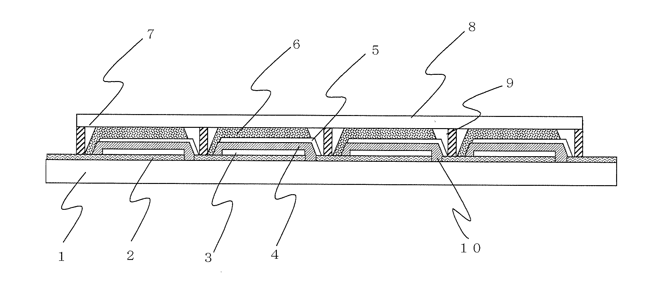
[0043]FIG. 1 is a schematic cross sectional view showing the layer configuration of main parts of a solar cell (Embodiment 1-1) of the present invention.
[0044]This solar cell is of a type having a second conductive layer 5 formed on a porous insulating layer 4, and specifically, the solar cell is provided with a conductive substrate A obtained by forming a first conductive layer 2 on a substrate 1; a catalyst layer 3, a porous insulating layer 4, a second conductive layer 5, a porous semiconductor layer 6 adsorbing a sensitizing dye, and a translucent cover member 8 formed subsequently on the first conductive layer 2, and the porous insulating layer 4 and the porous semiconductor layer 6 each contain an electrolyte 7. Further, a sealing part 9 is formed in the outer circumferential parts between the conductive substrate A and the translucent cover member 8.
[0045]The first conductive layer 2 has a scribe line 10 formed by removing a portion of the layer in the inside region near the ...
embodiment 1-2
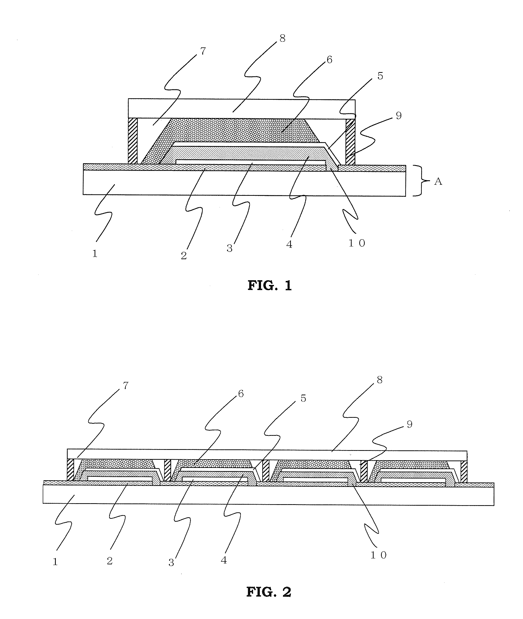
[0130]FIG. 2 is a schematic cross sectional view showing the layer configuration of main parts of a solar cell module (Embodiment 1-2) obtained by electrically connecting in series a plurality of solar cells (Embodiment 1-1) of the present invention.
[0131]This solar cell module can be produced as follows.
[0132]First, a first conductive layer formed on a substrate 1 is patterned by a laser scribing method at prescribed intervals to form a plurality of scribe lines in which the conductive layer is removed. Therefore, a plurality of mutually electrically separated first conductive layers 2 are formed and solar cell formation regions are provided on the respective first conductive layers 2.
[0133]Among the plurality of the first conductive layers 2, the first conductive layer 2 at one end in the direction perpendicular to the scribe lines 10 is formed to have a smaller width, and no solar cell is formed on the first conductive layer 2 with the smaller width. This first conductive layer 2...
embodiment 2-1
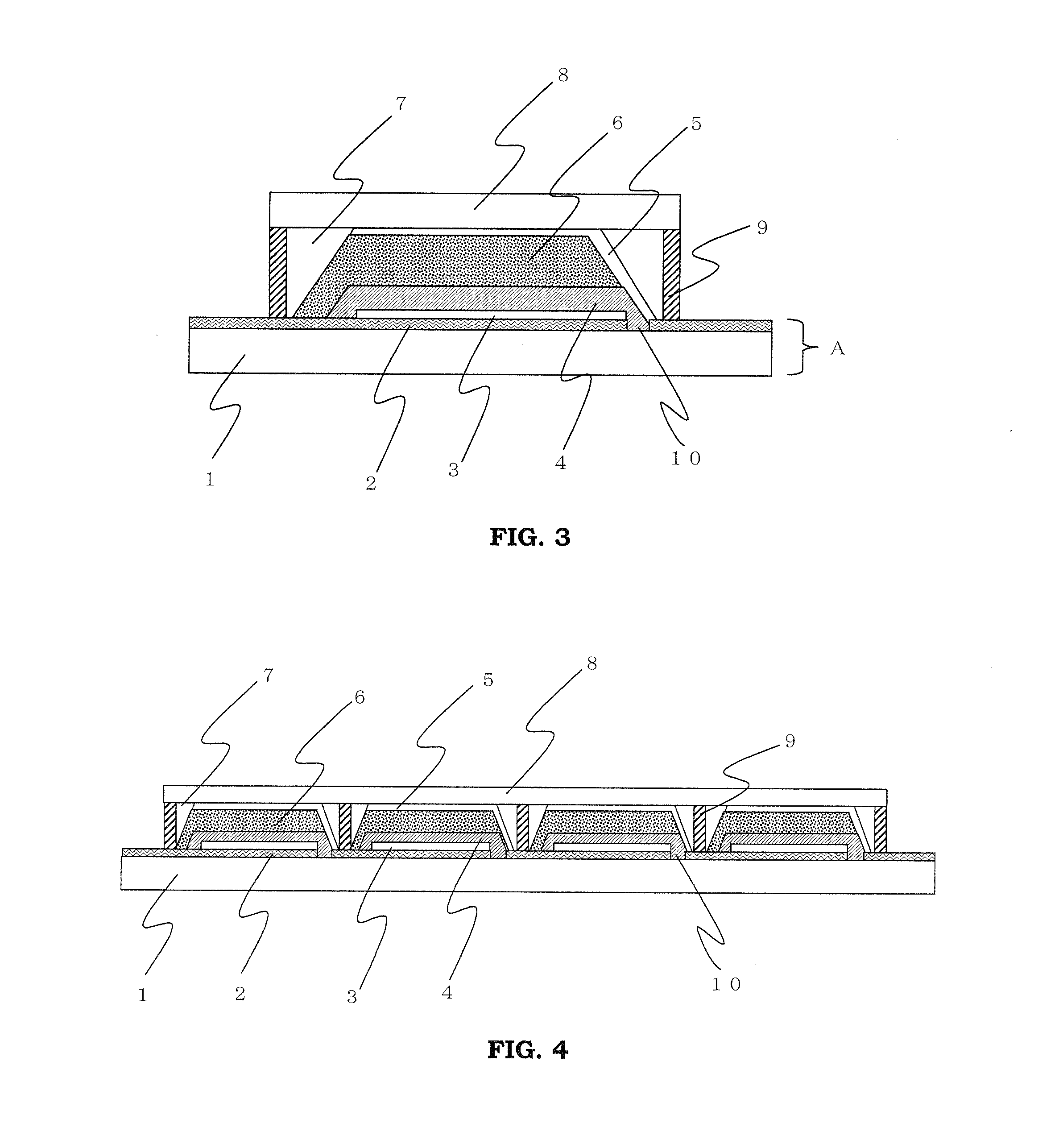
[0140]FIG. 3 is a schematic cross sectional view showing the layer configuration of main parts of a solar cell (Embodiment 2-1) of the present invention.
[0141]This solar cell is of a type in which the porous semiconductor layer 6 is formed on the porous insulating layer 4 in Embodiment 1-1 and the second conductive layer 5 is formed on the porous semiconductor layer 6, which is approximately same as that of Embodiment 1-1, except that the porous semiconductor layer 6 is formed on the porous insulating layer 4 so as to stride over the extracting electrode and that the second conductive layer 5 is formed on the porous semiconductor layer 6 so as to stride over the narrower first conductive layer 2. In this solar cell, since the second conductive layer 5 is formed on the porous semiconductor layer 6, the surface roughness coefficient Ra of the porous semiconductor layer 6 is equal to the surface roughness coefficient Ra of the interface of the porous semiconductor layer and the second ...
PUM
 Abstract
Description
Claims
Application Information