
Semiconductor Device Structure and Method for Manufacturing the same

Active Publication Date: 2012-02-23
INST OF MICROELECTRONICS CHINESE ACAD OF SCI
View PDF8 Cites 24 Cited by
  • Summary
  • Abstract
  • Description
  • Claims
  • Application Information

AI Technical Summary

Benefits of technology

[0030]According to the present invention, it is provided a method for forming source / drain regions in a self-aligned manner by means of performing implantation on a semiconductor substrate before forming the channel region and the gate stack, which achieves the advantageous effects of the replacement gate process without using the sacrificial gate, thereby simplifying the process and reducing the cost. In addition, performing the source / drain implantation before forming the channel region can avoid the diffusion of impurities which is likely to be caused by forming the source / drain regions in the conventional process. Meanwhile, by adding an inner sidewall spacer of the gate, the feature size of the channel under the gate can be effectively adjusted. Furthermore, the performance of an MOSFET device is greatly enhanced by applying an epitaxial channel that effectively increases the carrier mobility. In addition, one embodiment of the present invention also incorporates a particular process of gate electrode stripe cutting, which can effectively improve the isolation between the gate electrodes, simplify etching and photolithography of the gate electrodes, and reduce the difficulty in OPC (Optical Proximity Correction). This process is also compatible with the high-k dielectric / metal gate process.
[0031]Additional aspects and advantages of the present invention will be given in the following descriptions, some of which will be apparent from the following descriptions or be learned from practices of the present invention.

Problems solved by technology

However, said process has the following problems: the replacement gate process is complicated and has a high cost; it is more and more difficult to integrate contact holes into a CMOSFET (Complementary Metal Oxide Semiconductor Field Effect Transistor); and it is becoming harder to realize the high-k dielectric / metal gate stack process in a CMOS device.

Method used


Image

  • Semiconductor Device Structure and Method for Manufacturing the same
  • Semiconductor Device Structure and Method for Manufacturing the same
  • Semiconductor Device Structure and Method for Manufacturing the same

Examples


Embodiment Construction

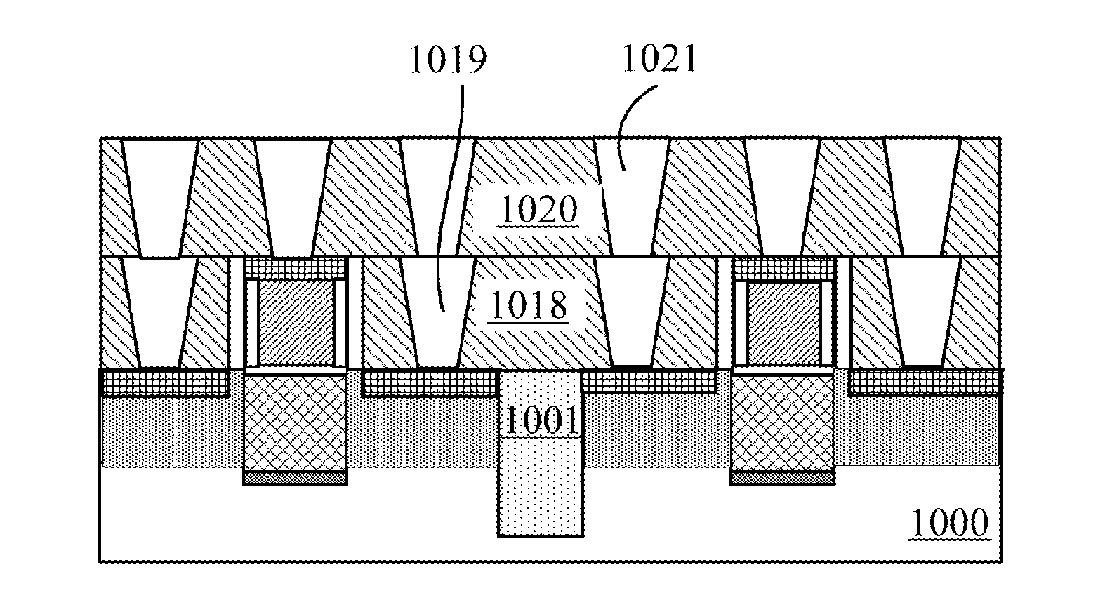
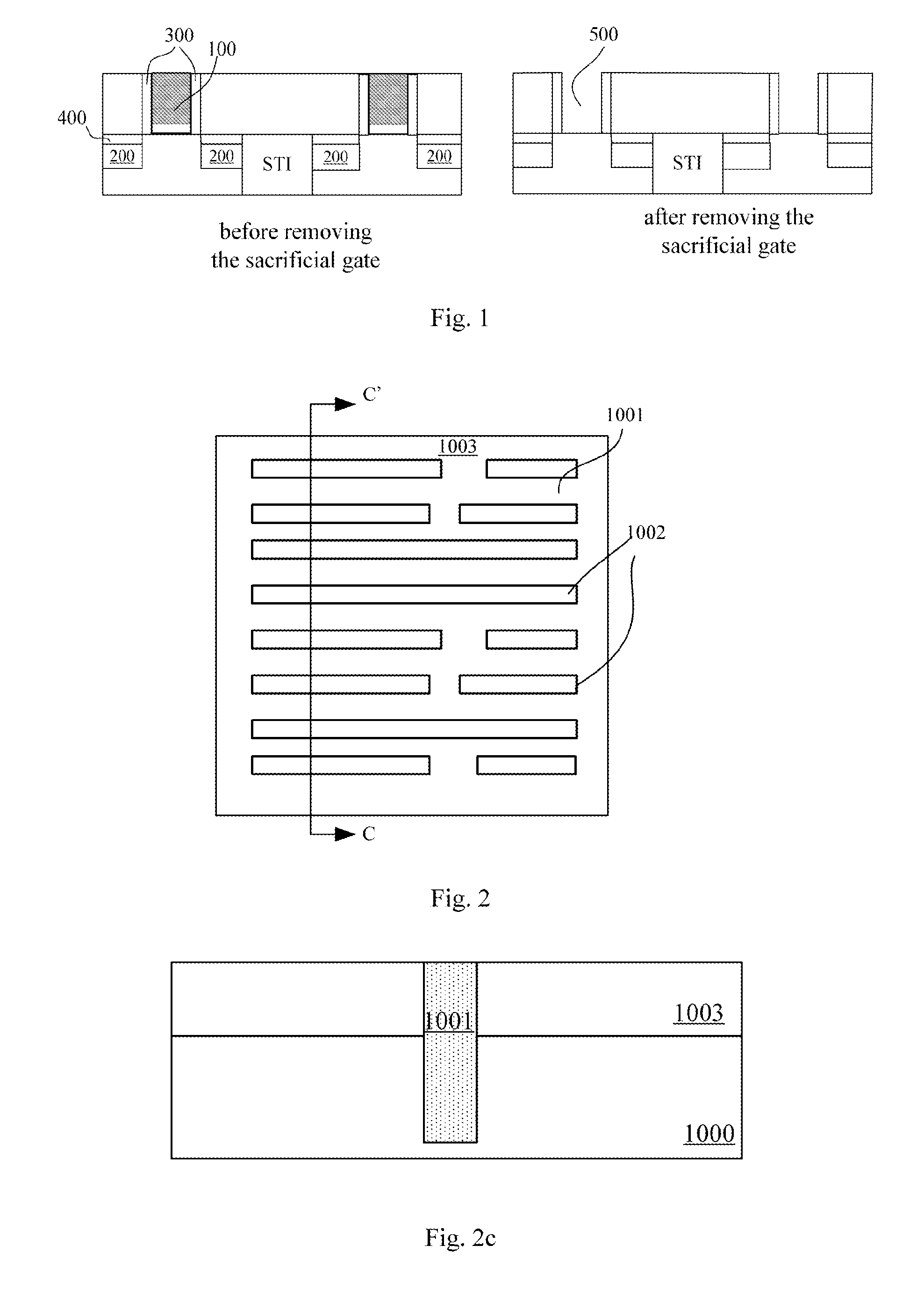
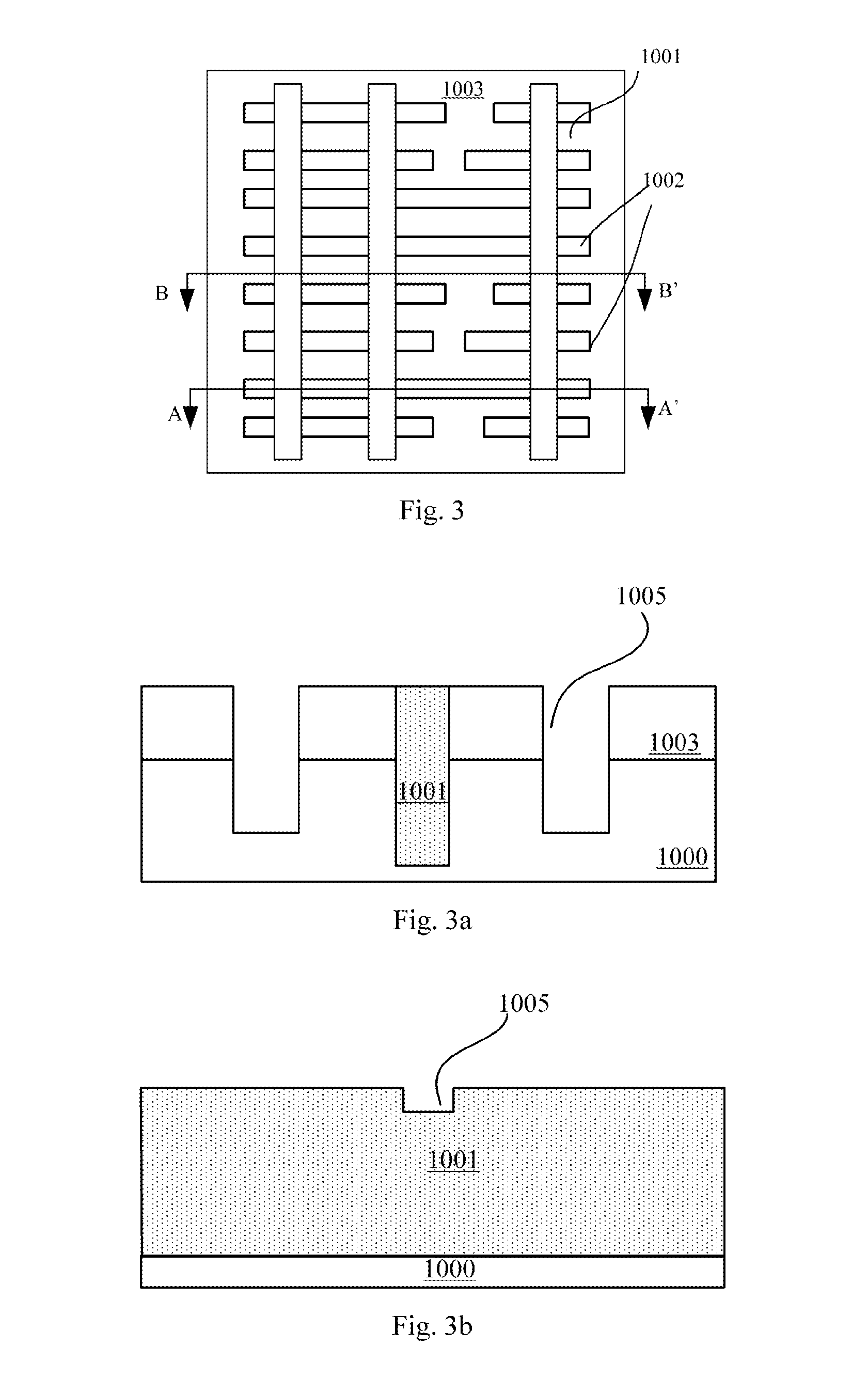
[0036]The embodiments of the present invention will be described in details below, and examples of said embodiments are shown in the figures. Throughout the drawings, the same or similar reference numbers represent the same or similar elements or elements having the same or similar functions. The embodiments described below with reference to the drawings are exemplary, which are only for illustrating the present invention instead of limiting the present invention.

[0037]The following disclosure provides a plurality of different embodiments or examples to achieve different structures of the present invention. To simplify the disclosure of the present invention, description of the components and arrangements of specific examples is given below. Of course, they are only illustrative and not intended to limit the present invention. Moreover, in the present invention, reference numbers and / or letters may be repeated in different embodiments. Such repetition is for the purposes of simplifi...


PUM


Abstract

The present invention presents a method for manufacturing a semiconductor device structure as well as the semiconductor device structure. Said method comprises: providing a semiconductor substrate; forming a first insulating layer on the semiconductor substrate; forming a shallow trench isolation embedded in the first insulating layer and the semiconductor substrate; forming a channel region embedded in the semiconductor substrate; and forming a gate stack stripe on the channel region. Said method further comprises, before forming the channel region, performing a source / drain implantation on the semiconductor substrate. By means of forming the source / drain regions in a self-aligned manner before forming the channel region and the gate stack, said method achieves the advantageous effects of the replacement gate process without using a dummy gate, thereby simplifying the process and reducing the cost.

Description

FIELD OF THE INVENTION[0001]The present invention relates to the technical field of semiconductor device design and manufacture, in particular, to a CMOS device in which source / drain regions are formed in a self-alignment manner before the formation of gate and a method for manufacturing the same.BACKGROUND OF THE INVENTION[0002]With the development of the semiconductor technology, the requirements on the performance and feature size of CMOS (Complementary Metal Oxide Semiconductor) devices are increasingly high. For the process integration of 45 nanometers technology node and below, the replacement gate (gate last) process is applied widely. FIG. 1 is a schematic drawing showing a typical conventional gate last process, which includes forming a sacrificial gate 100 first, forming source / drain regions 200, a sidewall spacer 30, and a silicide layer 400 covering the source / drain regions, then removing the sacrificial gate 100 to form an opening 500 surrounded by the inner walls of th...

Claims


Application Information

Patent Timeline
IPC IPC(8): H01L29/772H01L21/336
CPCH01L21/823814H01L21/823828H01L21/823878H01L27/0207H01L29/7848H01L29/66545H01L29/66553H01L29/66651H01L29/1054H01L29/66575H01L29/78H01L21/76224H01L29/0649H01L29/66477H01L29/7833H01L21/823412
Inventor ZHONG, HUICAILIANG, QINGQING
Owner INST OF MICROELECTRONICS CHINESE ACAD OF SCI
Learn More