
Semiconductor device

Active Publication Date: 2012-02-23
RENESAS ELECTRONICS CORP
View PDF1 Cites 34 Cited by
  • Summary
  • Abstract
  • Description
  • Claims
  • Application Information

AI Technical Summary

Benefits of technology

[0016]However, in the method of storing the ID as described above, a dedicated process is required, and therefore, its cost is increased. Also, there is a problem of a risk such that a data written at the manufacturing is falsified at practical using.
[0023]By using the semiconductor device according to the present invention, a memory which can be used for a normal function operation can be used for generating an ID, so that an area overhead does not occur.
[0024]Also, by using the semiconductor device according to the present invention, multiple bit for a bit length for identification in a SoC and a microcomputer on which a large number of memories are mounted can be easily achieved. As a result, weakness of a chip can be improved.

Problems solved by technology

However, in the method of storing the ID as described above, a dedicated process is required, and therefore, its cost is increased.
Also, there is a problem of a risk such that a data written at the manufacturing is falsified at practical using.
Therefore, its cost is increased due to increases in an area overhead and the number of pins.
Still further, since the dedicated hard macro is used, a bit length for identification is limited.

Method used


Image

  • Semiconductor device
  • Semiconductor device
  • Semiconductor device

Examples


first embodiment

[0056]FIG. 4 is a conceptual diagram showing a basic concept of an operation according to a first embodiment of the present invention. And, FIG. 5 is a diagram showing an example in generating a chip-unique ID according to the first embodiment of the present invention.

[0057]In the present invention, a fact that an error is caused by gradually decreasing an operation voltage of a transistor in a chip is used for generating the chip-unique ID. Note that a dynamic chip such as a DRAM is assumed here.

[0058]As clearly seen from FIG. 4, as long as a non-defective product, all transistors perform a normal operation when a standard voltage is applied to the transistors in a chip. Note that the standard voltage is a power supply voltage used for the normal operation, and the normal operation is a state in which a power supply voltage used for memory reading / updating operation is applied as assumed in a case that a non-defective information storage medium such as a non-defective DRAM is mount...

second embodiment

[0124]Next, a second embodiment of the present invention is described with reference to figures.

[0125]The first embodiment of the present invention describes the basic operation of the present invention. However, in the acquisition of the fail bit map which is easily executed by the description of the flowchart, there is a high possibility that a reproducibility problem arises in, more particularly, the SRAM. Accordingly, improvement of the reproducibility of the fail bit map is described.

[0126]Further, in the present embodiment, improvement of reproducibility of the fail bit map by adjusting an assist level of the SRAM is discussed.

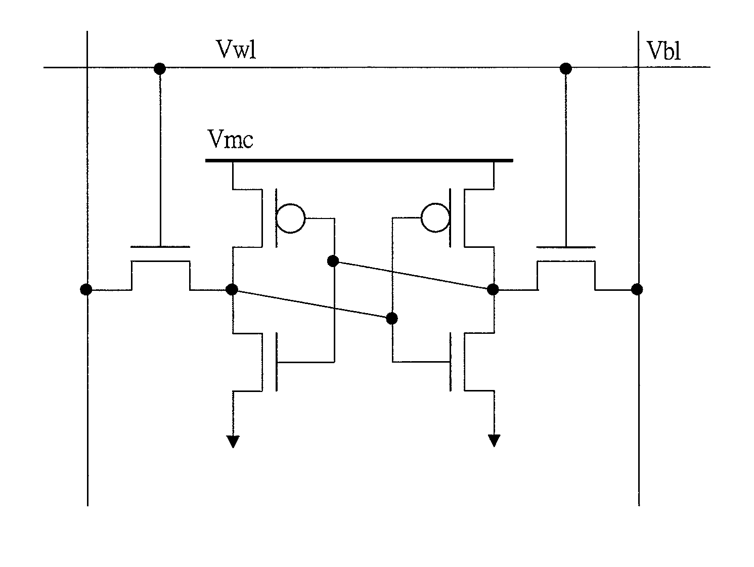
[0127]FIG. 10 is a circuit diagram showing the SRAM and voltages targeted for adjusting the assist level according to the second embodiment of the present invention.

[0128]First, the basic structure of the SRAM is described.

[0129]To this SRAM, three voltages are supplied. That is, they are a word-line potential Vwl, a bit-line potential Vbl, and a memory-...

third embodiment

[0148]Next, a third embodiment of the present invention is described.

[0149]In the first embodiment, as seen from FIG. 8, every time the verification request is issued, the memory BIST is operated to acquire the fail bit map.

[0150]By contrast, the present embodiment has a feature of using the data retained in the memory cell at power-on time as the chip-unique ID.

[0151]The data retained in the memory cell at the power-on time is determined by the random variation of the transistors of the memory cell. This value is retained in an arbitrary location in the memory, and is outputted when the verification request is issued, so that the reproducibility of the acquired data is improved. This is because it is not required to change the power supply voltage as different from the steps S1101 and S1105 (see FIG. 8).

[0152]However, the following points should be noted.

[0153]When the memory-line potential Vmc and the word-line potential Vwl (see FIG. 10) are simultaneously applied, there is a pos...


PUM


Abstract

By using a fact that a bit error in an on-chip embedded memory occurs at a random address, means for creating a chip-unique ID and utilizing this ID are provided. A controller having received a verification request from outside instructs a variable power supply circuit to decrease a voltage supplied to a memory to be lower than that at the normal operation time. When the voltage supplied to the memory is stabilized, the controller requests a memory test to a memory BIST. By using an address where an error occurs due to a result of the memory test, the controller creates the chip-unique ID and uses the ID as a response to the verification request.

Description

CROSS-REFERENCE TO RELATED APPLICATION[0001]The present application claims priority from Japanese Patent Application No. 2010-186040 filed on Aug. 23, 2010, the content of which is hereby incorporated by reference into this application.TECHNICAL FIELD OF THE INVENTION[0002]The present invention relates to verification of a semiconductor device. More particularly, the present invention relates to a verification test by a hardware on which dedicated processes are implemented as less as possible.BACKGROUND OF THE INVENTION[0003]A market of an electronic commerce service via the Internet such as e-commerce and net banking has steadily expanded. Also, an electronic money service using an IC card has entered into spread / expansion period. And, in these services, a higher-leveled security technique is always demanded.[0004]In a software level, sufficient security has been achieved by an encryption technique with a central focus on strong encryption algorithm. On the other hand, in a hardwar...

Claims


Application Information

Patent Timeline
IPC IPC(8): G11C7/00
CPCG11C29/44G11C16/20G11C7/24
Inventor FUJIWARA, HIDEHIRONII, KOJIYABUUCHI, MAKOTOARIMOTO, KAZUTAMI
Owner RENESAS ELECTRONICS CORP
Learn More