Dye-sensitized solar cell

a solar cell and dye sensitization technology, applied in the direction of electrolytic capacitors, sustainable manufacturing/processing, final product manufacturing, etc., can solve the problems of increasing the manufacturing cost of the cell, reducing the absorption efficiency, and not obtaining dye which is capable of highly efficient light absorption from 400 nm to a wavelength of near-infrared or longer wavelength, etc., to achieve excellent light absorption efficiency and reduce the manufacturing cost of the dye sensitized solar cell.

Inactive Publication Date: 2012-03-01
NAT UNIV CORP KYUSHU INST OF TECH (JP) +1
View PDF4 Cites 14 Cited by
  • Summary
  • Abstract
  • Description
  • Claims
  • Application Information

AI Technical Summary

Benefits of technology

[0028]The dye-sensitized solar cell according to the present invention is configured such that a first dye-carrying porous oxide semiconductor layer, a first electrolyte layer, and a cathode substrate are provided in order from the light incident side, such that an anode substrate is provided, or a transparent substrate in place of the anode substrate and further a porous conductive metal layer are provided, and such that an electrolyte redox catalyst layer, a second dye-carrying porous oxide semiconductor layer, a porous support layer, and the second electrolyte layer are further provided, or a second dye-carrying porous oxide semiconductor layer, a porous conductive metal support layer, and the second electrolyte layer are further provided. Thus, the dye-sensitized solar cell according to the present invention has an excellent light absorption efficiency. Further, since the dye-sensitized solar cell according to the present invention does not necessarily need an expensive transparent conductive film or does not need to use many expensive transparent conductive films, it is possible to reduce the manufacturing cost of the dye-sensitized solar cell.

Problems solved by technology

That is, various dyes for use in the dye-sensitized solar cell have hitherto been studied, but a dye which is capable of highly efficiently absorbing light of a wide wavelength range from a wavelength of 400 nm to a near-infrared or longer wavelength has not been obtained.
Note that, in order to improve the light absorption efficiency, it can be considered to increase the thickness of the porous semiconductor layer adsorbing the dye, but in this case, the increase in the thickness of the porous semiconductor layer does not actually lead to an improvement in the absorption efficiency due to various reasons, and on the contrary, the absorption efficiency may be reduced.
However, any of the above-described conventional techniques is considered to still have large room for further improvement, in view of such drawbacks as that the light absorption efficiency of the cell needs to be further improved, that the manufacturing cost of the cell is increased due to the use of many expensive transparent conductive films in the cell structure, or that a problem may be caused when the size of the cell is increased.

Method used


Image

  • Dye-sensitized solar cell
  • Dye-sensitized solar cell
  • Dye-sensitized solar cell

Examples


example 1

Manufacturing Example 1 of Dye-Sensitized Solar Cell According to First Example of Present Embodiment

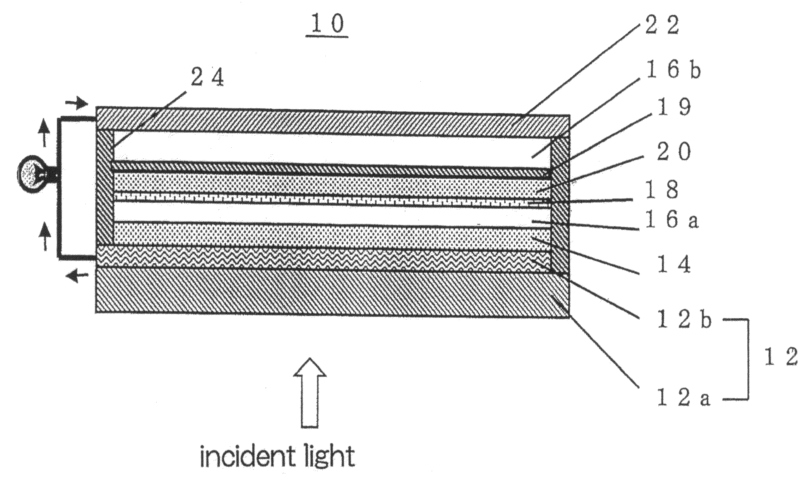
[0085]An FTO film (surface resistance: 10Ω / □) is formed on a transparent glass substrate. Further, a titania paste is applied on the FTO film and then dried at 450° C. for 30 minutes, so that a porous titania layer having a thickness of 2 μm is manufactured. The first electrode section is manufactured by making the first dye (Dye2) adsorbed in the porous titania layer. On the other hand, a titanium film is formed by sputtering titanium on a mesh stainless steel substrate (thickness: 25 μm) having a mesh of 20 μm diameter, and then a titanium film is further formed by an arc plasma method while introducing oxygen, so that a stainless steel mesh structure having a protected surface is manufactured. A titania paste is applied to the surface of one side of the mesh structure, and then dried at 450° C. for 30 minutes, so that a porous titania layer having a thickness of 2 μm is manufactur...

example 2

Manufacturing Example 2 of Dye-Sensitized Solar Cell According to First Example of Present Embodiment

[0086]An FTO film (surface resistance: 10Ω / μ) is formed on a transparent glass substrate. Further, a titania paste is applied on the FTO film, and then dried at 450° C. for 30 minutes, so that a porous titania layer having a thickness of 2 μm is manufactured. The first electrode section is manufactured by making the first dye adsorbed in the porous titania layer. On the other hand, a titanium film is formed by sputtering titanium on a mesh stainless steel substrate (thickness: 25 μm) having a mesh of 20 μm diameter, and then a titanium film is further formed by an arc plasma method while introducing oxygen, so that a stainless steel mesh structure having a protected surface is manufactured. A titania paste is applied to the surface of one side of the mesh structure, and then dried at 450° C. for 30 minutes, so that a porous titania layer having a thickness of 2 μm is manufactured. Th...


PUM


Abstract

To provide a tandem dye-sensitized solar cell having a novel structure capable of improving the light absorption efficiency and being manufactured less expensively. A dye-sensitized solar cell 10 is configured by including, in order from the light incident side, an anode substrate 12, a first dye-carrying porous oxide semiconductor layer 14, a first electrolyte layer 16a, an electrolyte redox catalyst layer 18, a second dye-carrying porous oxide semiconductor layer 20, a porous support layer 19, a second electrolyte layer 16b, and a cathode substrate 22. The electrons extracted from a conductor layer 12b by a conductor are introduced into the cathode substrate 22, so that a battery circuit, for example, for a lighting power source is configured.

Description

BACKGROUND OF THE INVENTION[0001]1. Field of the Invention[0002]The present invention relates to a so-called tandem dye-sensitized solar cell in which porous oxide semiconductor layers carrying dyes are arranged in series along a propagation direction of incident light.[0003]2. Description of the Related Art[0004]A dye-sensitized solar cell is referred to as a wet-type solar cell or a Graetzel cell, and is featured by including an electrochemical cell structure which is composed typically of an iodine solution without using a silicon semiconductor. Specifically, the dye-sensitized solar cell has a simple structure in which an iodine solution, or the like, is arranged, as an electrolyte solution, between a porous semiconductor layer (porous oxide semiconductor layer), such as a titania layer, formed by baking titanium dioxide powder, or the like, onto a transparent conductive glass plate (a transparent substrate with a transparent conductive film laminated thereon: anode substrate) a...

Claims


Application Information

Patent Timeline
Patent Type & Authority Applications(United States)
IPC IPC(8): H01L31/06H01L51/44
CPCH01G9/2031H01G9/2059Y02E10/542H01L51/0064H01G9/2072Y02P70/50H10K85/652
Inventor HAYASE, SHUZIPANDEY, SHYAM S.YAMAGUCHI, YOSHIHIRO
Owner NAT UNIV CORP KYUSHU INST OF TECH (JP)
Why Eureka
Try Eureka