Graphene transparent electrode, graphene light emitting diode, and method of fabricating the graphene light emitting diode

a graphene light-emitting diode and graphene-based technology, applied in the direction of carbon-silicon compound conductors, electrical devices, semiconductor devices, etc., can solve the problems of difficult to obtain excellent black screen, inability to efficiently increase the brightness of lcds, and difficulty in obtaining excellent black screen, etc., to achieve better electrical resistance, improve the effect of transparency and lower thickness

Inactive Publication Date: 2012-03-01
SUNG CHIEN MIN
View PDF6 Cites 33 Cited by
  • Summary
  • Abstract
  • Description
  • Claims
  • Application Information

AI Technical Summary

Benefits of technology

[0009]According to the present invention, the graphene sheets of the graphene transparent electrode have a two-dimensional structure with large area. The graphene transparent electrode of the present invention can serve as a transparent electrode and can be applied to various optical devices such as LCD, OLED, or solar cell, or other electronic devices. The graphene transparent electrode of the present invention comprises graphene sheets overlapping with each other, the transparency of the graphene transparent electrode of the present invention is high (70% or above), the resistance is 1 Ω / cm or below (more preferably 10−4 Ω / cm or below), and therefore is able to replace the conventional transparent ITO electrode. The graphene transparent electrode of the present invention is advantageous in being thin and having low power consumption, which cannot be achieved with a conventional ITO transparent electrode.
[0027]The gLED made by the method of the present invention uses graphene as a raw material, and therefore the manufacturing cost can be largely lowered. Besides, due to a high transparency of the graphene sheets, the brightness of the gLED can be increased. Also, a longer lifespan can be achieved according to the gLED made by the method of the present invention compared with a conventional OLED. The gLED made by the method of the present invention also has advantages such as being ultra thin, with high chromaticity, and low power consumption, and therefore the gLED made by the method of the present invention is of high commercial value.

Problems solved by technology

However, those optical films may result in the decreasing of the light transmittance of the LCDs, whereby the brightness of the LCDs cannot be efficiently increased.
Besides, an LCD also has a disadvantage that an excellent black screen is hard to obtain, i.e. the light from the backlight source cannot be completely shielded with the liquid crystal displaying panel; hence light leakage may occur.
Therefore the contrast and the coloring performance of the LCD cannot be improved.
Moreover, long response time is also a technical problem hard to be solved in the LCD field.
However, the OLED projects still have some problem to be solved such as insufficient brightness (only 300 nit), short lifespan (less than 10,000 hours), and high manufacturing cost; furthermore, the thickness of the transparent electrode made of ITO not being able to be further reduced, which may result in an unfavorable light transmittance and electrical conductivity.

Method used


Image

  • Graphene transparent electrode, graphene light emitting diode, and method of fabricating the graphene light emitting diode
  • Graphene transparent electrode, graphene light emitting diode, and method of fabricating the graphene light emitting diode
  • Graphene transparent electrode, graphene light emitting diode, and method of fabricating the graphene light emitting diode

Examples


example 1

The Providing of Graphite Film Comprising Plural Layered Graphene Sheets

[0047]The graphite film of the present example is made by a solid state method as described below.

[0048]First, a pure graphite powder is coated on a quartz substrate and then the quartz substrate coated with the graphite powder is placed in a tube-shape in a vacuum degree of 10−5 Torr.

[0049]Then, the quartz substrate coated with the graphite powder is heat treated at a temperature of 1200° C. to form a graphite film. After cooling, the formed graphite film is taken off from the quartz substrate to obtain the graphite film comprising plural of layered graphene sheets of the present example.

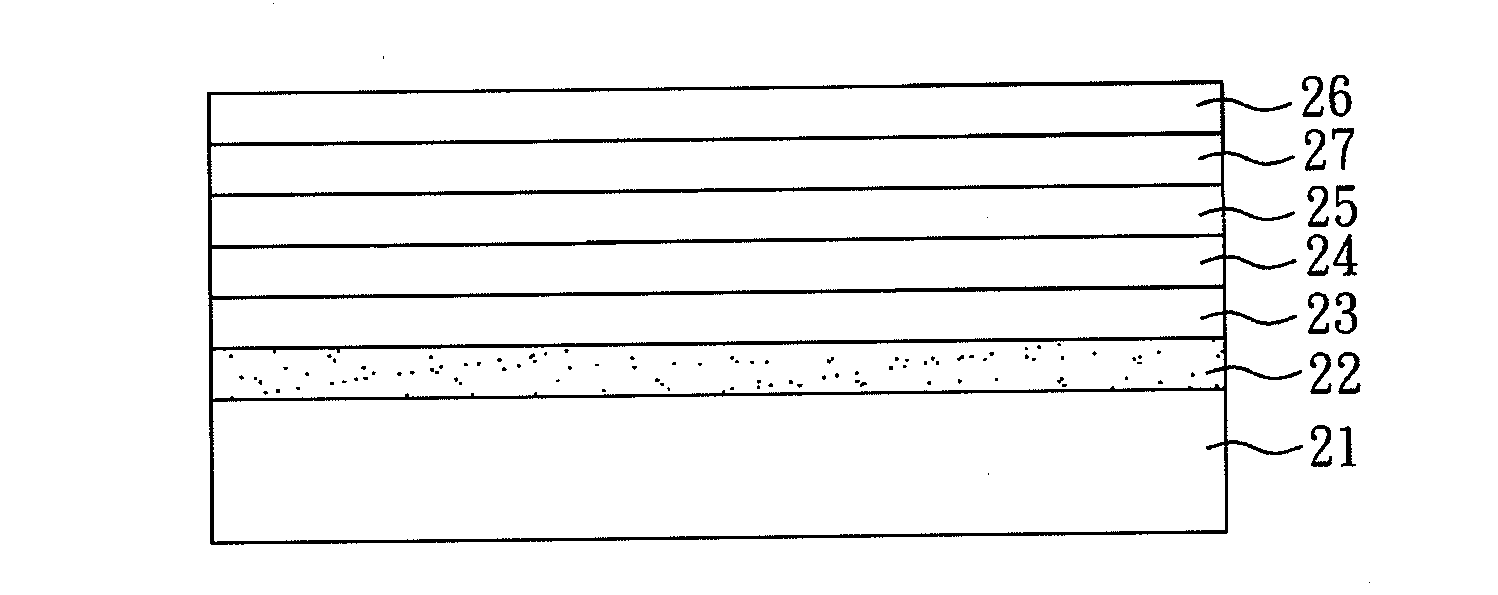
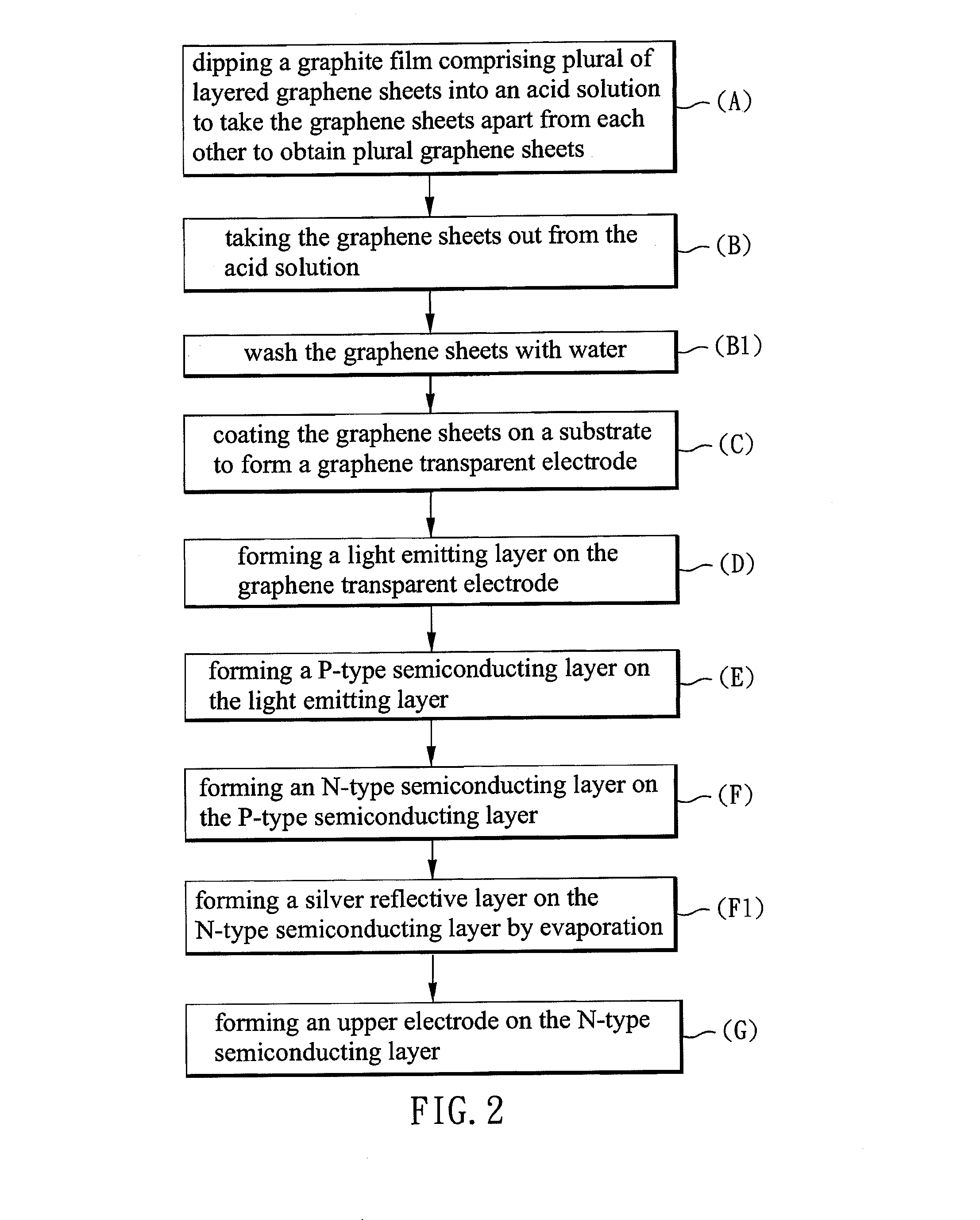
[0050]The Providing of Graphene Light Emitting Diode

[0051]Reference with FIG. 2, a process flow chart of fabricating a gLED of the present example is shown. First, (A) the graphite film comprising plural of layered graphene sheets formed above is dipped into a sulfuric acid solution to separate the graphene sheets from each oth...

example 2

[0059]The same method as described in the example 1 is used here to provide a gLED of the present example, except that an aromatic tertiary amine compound is used to form the P-type semiconducting layer.

[0060]The P-type semiconducting layer, the light emitting layer, and the N-type semiconducting layer in the gLED of the present invention can be made of materials that are used in a conventional OLED. The materials used in the example 1 are most proper, but are not limited thereto.

example 3

[0061]The same method as described in the example 1 is used here to provide a gLED of the present example, except that a plastic substrate is used as the substrate herein.

[0062]The plastic substrate herein may be a flexible substrate, thus the gLED made in the present example is a flexible gLED.


PUM

PropertyMeasurementUnit
light transmittanceaaaaaaaaaa
diameteraaaaaaaaaa
thicknessaaaaaaaaaa

Abstract

A graphene transparent electrode, which comprises: at least one graphene sheet; wherein the graphene sheets electrically connect with each other by overlapping with each other, each of the graphene sheets has a diameter from 10 μm to 1 mm, the quantity of the graphene sheets in the graphene transparent electrode is from 1 to 1000, the electrical resistance of the graphene transparent electrode is 1 Ω / cm or below, and the light transmittance of the graphene transparent electrode is 70% or above. A graphene light emitting diode (gLED) and a method of fabricating the same are also disclosed.

Description

BACKGROUND OF THE INVENTION[0001]1. Field of the Invention[0002]The present invention relates to a graphene transparent electrode, a graphene light emitting diode (gLED) comprising the same, and a method of fabricating the said gLED, more particularly, to a graphene transparent electrode comprising graphene sheets, a graphene light emitting diode (gLED) comprising the same, and a method of fabricating the said gLED.[0003]2. Description of Related Art[0004]In recent years, liquid crystal displays (LCD) have been applied as the displaying device for various electronics such as televisions or computer displays. For a liquid crystal display, a backlight source such as light-emitting diode (LED) or cold cathode fluorescent lamps (CCFL) should be used, because LCDs are not self-lighting devices. Also, optical films such as polarizer plates, light guide plates, or screen boards are used in a liquid crystal display. However, those optical films may result in the decreasing of the light tran...

Claims


Application Information

Patent Timeline
Patent Type & Authority Applications(United States)
IPC IPC(8): H01L33/36H01L21/28H01L29/167
CPCH01B1/04H01L29/1606H01L2251/5338H01L51/5206H01L51/5215H01L33/42H10K50/81H10K2102/311
Inventor SUNG, CHIEN-MIN
Owner SUNG CHIEN MIN
Why Eureka
Try Eureka