Ball grid array package

a technology of ball grid array and semiconductor, applied in the field of packaged semiconductor devices, can solve the problems of false soldering of solder balls, affecting the layout of high-density circuitry between the substrates, and thicker substrate thickness, so as to reduce the amount of power/ground metal layers disposed, thin semiconductor packages, and the effect of reducing the cost of the substra

Inactive Publication Date: 2012-03-01
POWERTECH TECHNOLOGY
View PDF10 Cites 5 Cited by
  • Summary
  • Abstract
  • Description
  • Claims
  • Application Information

AI Technical Summary

Benefits of technology

[0006]The main purpose of the present invention is to provide a BGA package structure to effectively reduce the power/ground metal layers disposed inside t

Problems solved by technology

However, as shown in FIG. 3, substrates with multiple layers have higher substrate cost and thicker substrate thickness.
Even though the electrical performance and heat dissipation can be enhanced, however, the heights and the surface tension of

Method used


Image

  • Ball grid array package
  • Ball grid array package
  • Ball grid array package

Examples


Embodiment Construction

[0022]With reference to the attached drawings, the present invention is described by means of the embodiment(s) below where the attached drawings are simplified for illustration purposes only to illustrate the structures or methods of the present invention by describing the relationships between the components and assembly in the present invention. Therefore, the components shown in the figures are not expressed with the actual numbers, actual shapes, actual dimensions, nor with the actual ratio. Some of the dimensions or dimension ratios have been enlarged or simplified to provide a better illustration. The actual numbers, actual shapes, or actual dimension ratios can be selectively designed and disposed and the detail component layouts may be more complicated.

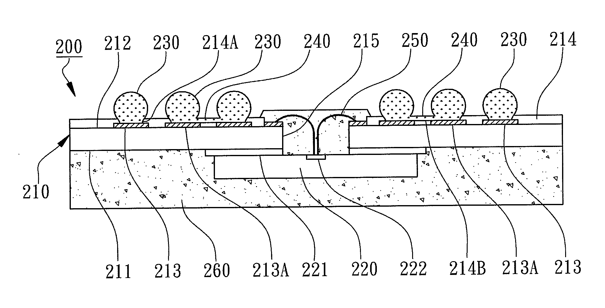
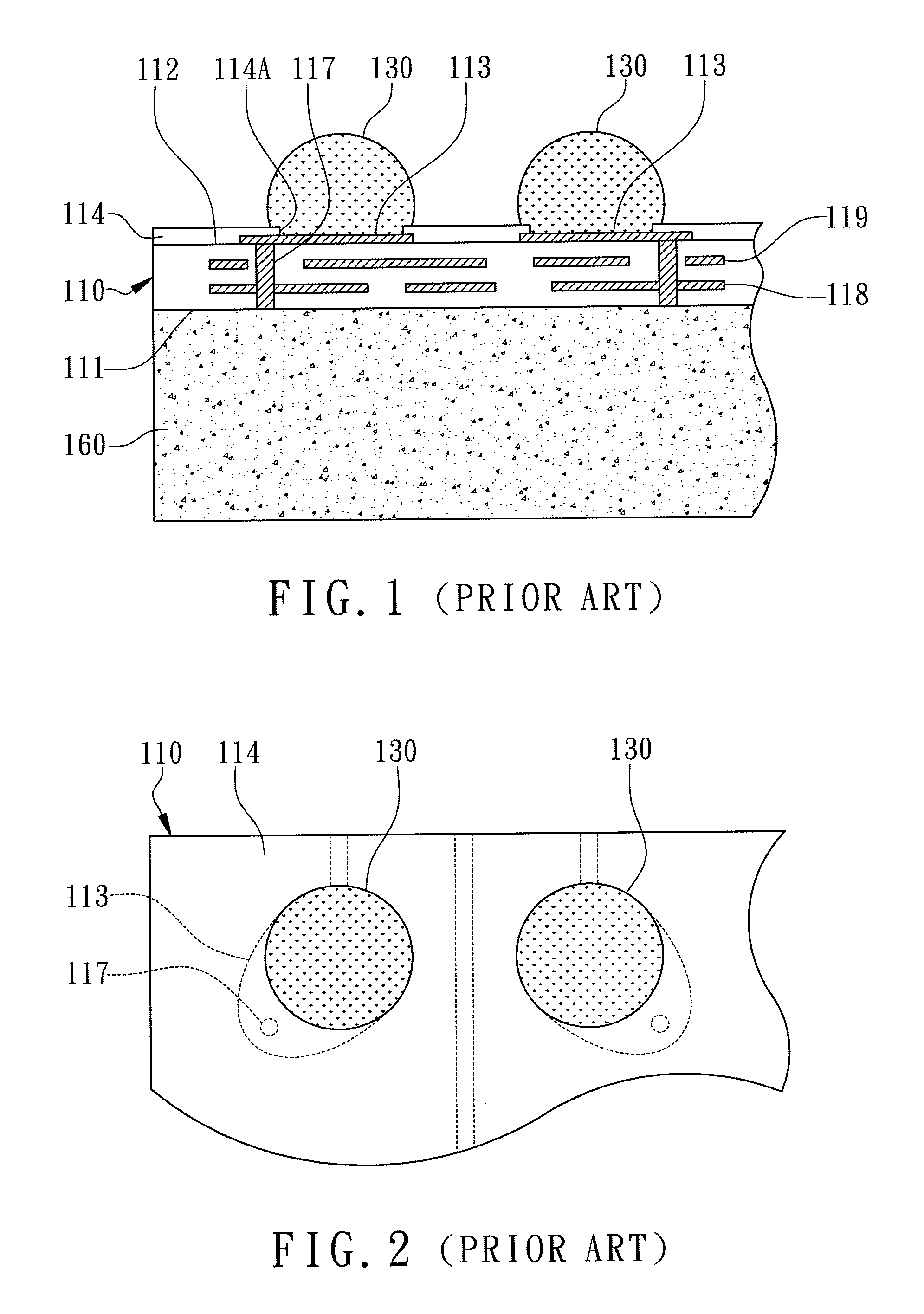
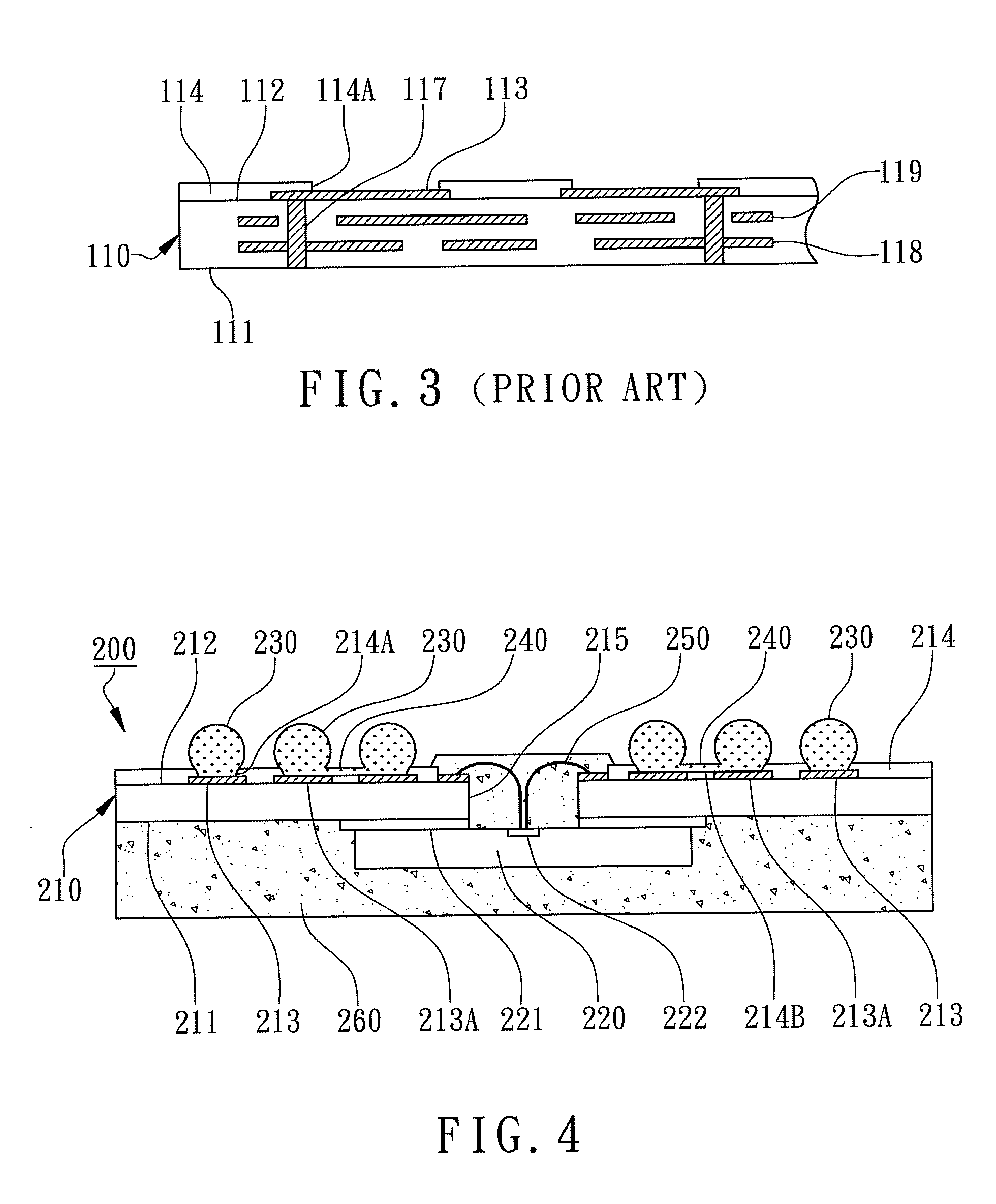
[0023]According to the first embodiment of the present invention, a BGA package is illustrated in FIG. 4 and FIG. 5 for cross-sectional views, FIG. 6 for a partial bottom view, and FIG. 7 for a partial three-dimensional botto...


PUM


Abstract

A BGA package comprises a substrate, a chip disposed on the substrate, and a plurality of solder balls disposed under the substrate. The substrate further has a plurality of ball pads and a solder mask having a plurality of openings to expose the ball pads where the ball pads include two or more non-signal pads. Solder mask further has a trench connecting the ones of the openings on the non-signal pads where the trench is filled with solder paste so that the solder balls bonded to the non-signal pads are electrically connected together to achieve power integrity and to reduce numbers of power/ground layers to make the package thinner and the substrate cost lower.

Description

FIELD OF THE INVENTION[0001]The present invention relates to packaged semiconductor devices, especially to BGA (Ball Grid array) packages.BACKGROUND OF THE INVENTION[0002]Ball grid array packages (BGA packages) are widely implemented in IC products with internally disposed semiconductor IC and with multiple-rows of solder balls arranged in an array to joint to an external printed circuit board having the advantages of smaller dimensions with high circuitry density when comparing to conventional packages with external leads extended from the encapsulant.[0003]There are four primary components of a BGA package: substrate, chip, encapsulant, and solder balls. One surface of the substrate is the joint surface for SMT and the other surface is the die-attaching surface for chip. Usually substrate is a printed circuit board with fine-pitch circuitry where multiple metal layers in substrate include different signal wiring layers, power plane, and ground plane which are designed and manufact...

Claims


Application Information

Patent Timeline
IPC IPC(8): H01L23/498
CPCH01L23/13H01L23/49816H01L23/49822H01L23/50H01L2224/16227H01L2224/4824H01L2224/73204H01L2224/73265H01L2924/15311H01L24/48H01L2224/16225H01L2224/32225H01L2224/48227H01L2224/48465H01L2224/73215H01L2224/45144H01L2224/45147H01L2224/05552H01L2224/48599H01L2224/48799H01L2924/30107H01L2224/0401H01L2924/00H01L2924/00012H01L2924/00014H01L24/45H01L24/73H01L2924/14H01L2924/181H01L2224/05599
Inventor FAN, WEN-JENG
Owner POWERTECH TECHNOLOGY
Why Eureka
Try Eureka