Sensor system with plasmonic nano-antenna array

a technology of plasmonic nanoantenna and array, which is applied in the direction of optical radiation measurement, instruments, spectrometry/spectrophotometry/monochromator, etc., can solve the problems of uncontrollable close-packed hexagonal structure, non-scalability of above-ground approaches, and inability to achieve scalability, etc., to achieve the effect of large local electromagnetic field enhancemen

Active Publication Date: 2012-03-01
LU WEIXING +1
View PDF1 Cites 38 Cited by
  • Summary
  • Abstract
  • Description
  • Claims
  • Application Information

AI Technical Summary

Benefits of technology

[0013]In order to provide the high sensitivity SERS active substrates needed for rapid and sensitive chemical / biological agent detection, the preferred embodiment of the present invention provides (1) a Plasmonic Nano-antenna Array (PNA) substrate with large local electromagnetic field enhancements; (2) a controllable and repeatable nano-fabrication process for creating the PNA surface; and (3) a system design for a compact, portable device capable of using the PNA technology to acquire and analyze target molecular samples.
[0014]The first embodiment of the present invention represents a key advance in the important field of Raman spectroscopy and nano-structure fabrication and will lead not only to greatly increased chemical detection capabilities but also to numerous new products to address a wide range of physical, chemical, medical and environmental sensor applications. The first embodiment of the present invention improves Raman sensor performance by constructing and applying a new type of substrate to the Raman sensor that possesses the required surface nano-architecture. The first embodiment also includes a low-cost method for nano-fabrication of the required substrates that is highly controllable, scalable, repeatable and low-cost. A first embodiment of the present invention will enable others to pursue the fabrication of nanostructures for many useful applications, such as super lenses, negative refractive index materials, meta-materials, plasmonic devices, enhanced optical transmitters, and equipment for plasmonic nano-lithography. An embodiment of the present invention has the potential to open up new sensor applications with corresponding new markets for U.S. industry.
[0015]INNOVATIONS OF THE PNA GAS SAMPLING SYSTEM: The technology has the following advantages over prior approaches:
[0016]Ultra-sensitivity: The innovative nano-antenna array based SERS active substrate significantly enhances signal strength by as much as 1014˜1015 times, elevating the system to single molecule sensing levels.
[0018]High reliability: The identification mechanism of the technology is based on fingerprints of target molecular conformation structures, by which false positive sensor readings can essentially be eliminated. The confidence of molecular identification also can be enhanced by the innovative sample collection mode (suck-in / adsorption / blow-out

Problems solved by technology

The above approaches for fabrication of plasmonic nano-antenna arrays require very expensive processes such as electron beam lithography, and electron beam evaporation and lift-off processes.
However, this approach suffers from non-scalability and is uncontrollable because the nanoparticle array is based on evaporation of a solvent from a single droplet resulting in an uncontrollable close-packed hexagonal structure.

Method used


Image

  • Sensor system with plasmonic nano-antenna array
  • Sensor system with plasmonic nano-antenna array
  • Sensor system with plasmonic nano-antenna array

Examples


first embodiment

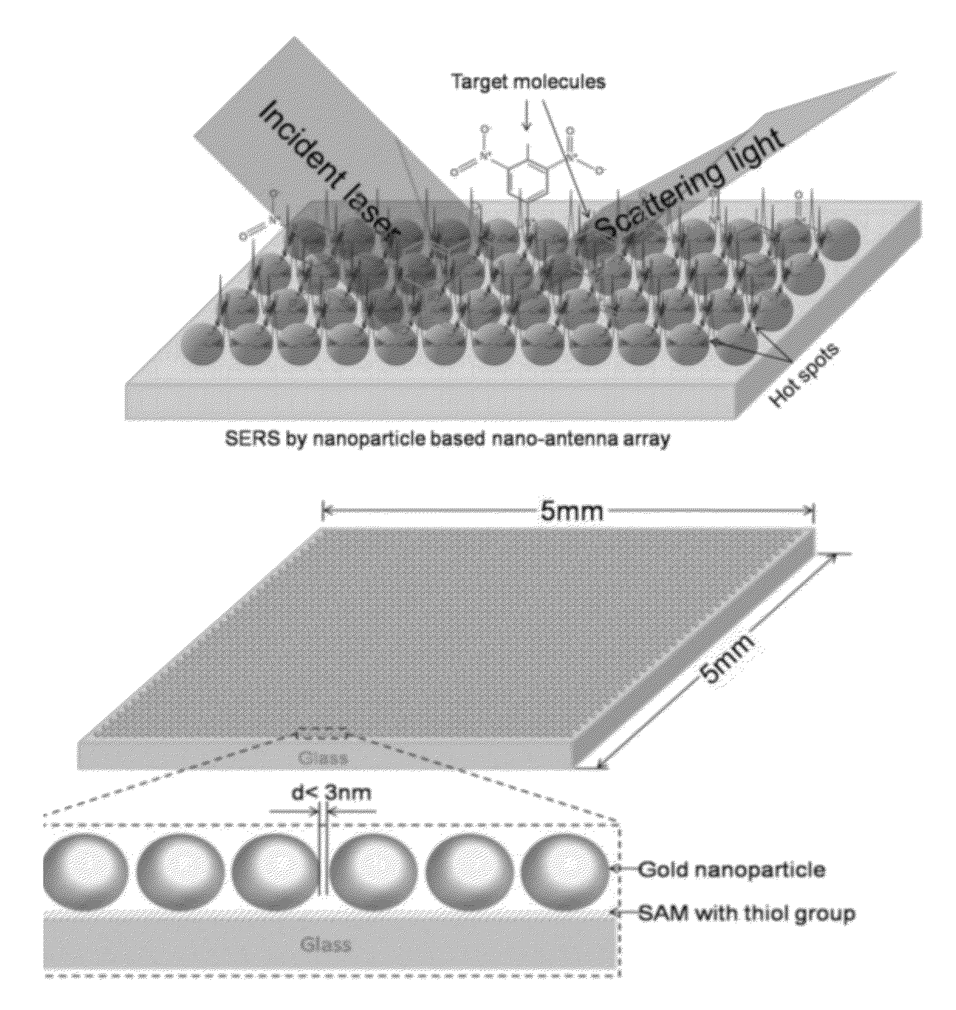
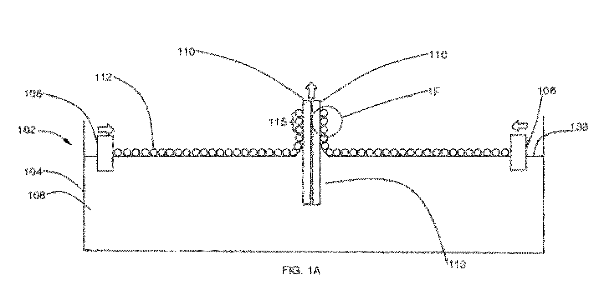
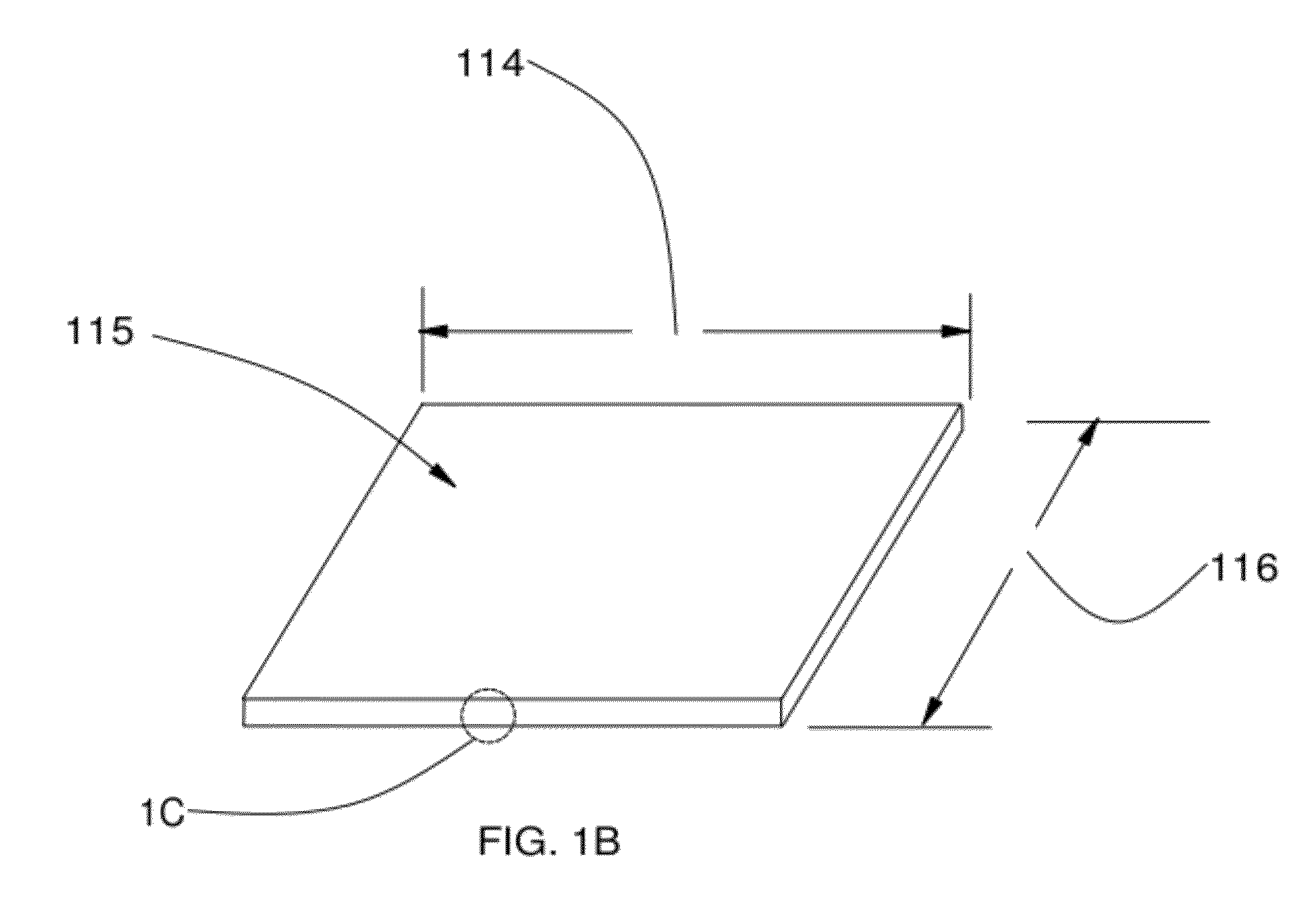
[0104]THE PLASMONIC NANO-ANTENNA 131 ARRAY (PNA) SUBSTRATE: FIGS. 1A through 1F schematically illustrate the basic process (FIG. 1A) and resulting plasmonic nano-antennae array structure (FIGS. 1B through 1F) of nano-antenna array substrate 111 produced by the water-filled Langmuir-Blodgett trough system 102. Such large-scale, highly SERS-active substrates can only be obtained by assembling a crystal-like nanoparticle array 115 on a solid substrate 110 such as glass, metal, acrylic, plastic, optical fiber core, or textile using a Langmuir-Blodgett Controlled Self-Assembly (LBCSA) fabrication technology. The nanoparticles are selected from gold (Au), Silver (Ag), Rhodium (Rh), Palladium (Pd), Osmium (Os), Iridium (Ir), Platinum (Pt), Titanium (Ti) or Aluminum (Al), or a combination of them. In the following, a two-trough Langmuir-Blodgett trough system is described, however the inventive concepts apply to single trough system also.

[0105]Again referring to FIGS. 1A through 1F, using t...

second embodiment

[0148]Multiple optical fibers with the deposited nano antennas can be combined to form an optical fiber bundle 202 as shown in FIG. 9D. Inside the gas sensor head of the second embodiment, the target gas sample molecules are drawn in and guided via a gas flow channel through the nano-antenna fiber optic bundle array 204 (FIG. 9C). Laser light is guided through the nano-antenna fiber optic bundle array on its way to the Raman spectrometer by employing a series of optical mirrors 196, optical lenses 198 and filters 200 (FIG. 9B).

[0149]The plasmonic nano antenna fiber optic bundle array increases the Raman scattering signal strength and also increase the probability of capturing the target molecules 124 in the antenna hot spots to nearly 100%. The excited hot spots fill the entire gas flow channel so that the passing target molecules cannot avoid interacting with them. The plasmonic nano-antenna array is assembled by parallel arrangement of the antennas on the optical fiber core surfac...


PUM


Abstract

In order to provide the high sensitivity SERS active substrates needed for rapid and sensitive chemical / biological agent detection, the present invention provides a Plasmonic Nano-antenna Array (PNA) substrate with large local electromagnetic field enhancements; a controllable and repeatable nano-fabrication process for creating the PNA surface; and a system design for a compact, portable device capable of using the PNA technology to acquire and analyze target molecular samples. Both 2D and 3D systems are provided.

Description

CROSS-REFERENCE TO RELATED APPLICATIONS[0001]This application claims the benefit of the U.S. Provisional Patent Application No. 61 / 377,082 filed Aug. 25, 2010 by the present inventors. This provisional patent application is incorporated herein in its entirety by reference.TECHNICAL FIELD[0002]The present invention relates generally to creating a specific nano-structure on a substrate to improve the sensitivity of surface enhanced Raman spectroscopy (SERS).BACKGROUND OF THE DISCLOSURE[0003]Certain chemical and biological contaminants can be harmful or dangerous at very low levels (low parts per billion (ppb) for chemicals and 1-100 cts / ml for biological agents) and, therefore, a rapid and sensitive detection of such toxins and pollutants in air and drinking water, followed by rapid remediation, is critically important. However, many biological and chemical materials such as explosives, protein biotoxins and some microbial materials cannot be detected by current methods such as bindin...

Claims


Application Information

Patent Timeline
Patent Type & Authority Applications(United States)
IPC IPC(8): G01J3/44B05D1/36B05D3/00B82Y20/00B82Y40/00
CPCB05D1/204B82Y10/00G01N21/658B82Y30/00B82Y40/00B82Y20/00
Inventor LU, WEIXINGROBERTS, ALLAN
Owner LU WEIXING
Why Eureka
Try Eureka