

Method for designing semiconductor device
a technology for semiconductor devices and design methods, applied in individual semiconductor device testing, semiconductor/solid-state device testing/measurement, instruments, etc., can solve the problems of difficult to completely remove moisture from the semiconductor device, difficult to completely prevent the entry of moisture from the air, and the reliability of the semiconductor device has degraded, so as to achieve high reliability and high-reliability light-emitting
- Summary
- Abstract
- Description
- Claims
- Application Information
AI Technical Summary
Benefits of technology
Problems solved by technology
Method used
Image

Examples
embodiment 1
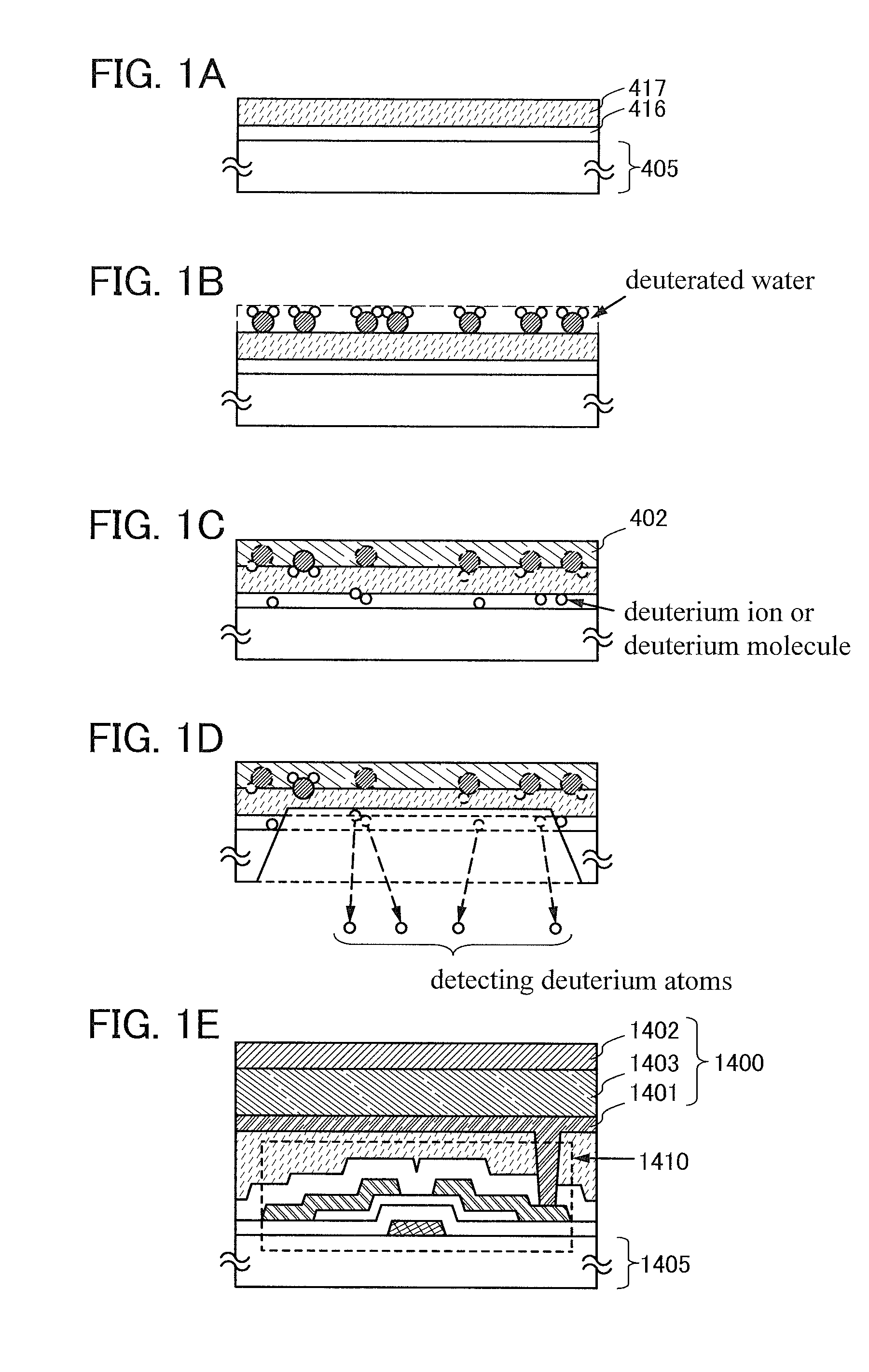
[0041]In this embodiment, a stacked layer of a silicon oxide film and an organic film is provided over a substrate, the organic film is coated with deuterated water, and then a conductive film is formed in contact with the organic film. Next, an inert conductive material that reacts with deuterated water to a degree that does not easily allows generation of a deuterium ion or a deuterium molecule is selected by measuring the amount of deuterium that exists in the silicon oxide film. Further, a method for designing a semiconductor device will be described with reference to FIGS. 1A to 1E. The semiconductor device includes a first electrode electrically connected to a source electrode layer or a drain electrode layer of an enhancement transistor including an oxide semiconductor in a channel formation region, and an organic layer containing a light-emitting substance provided between the first electrode and a second electrode overlapped with the first electrode. A conductive film inclu...
embodiment 2
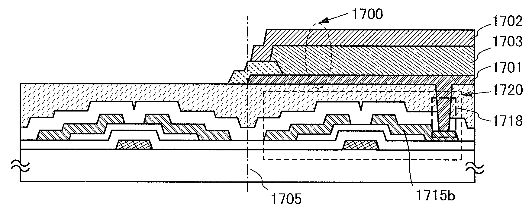
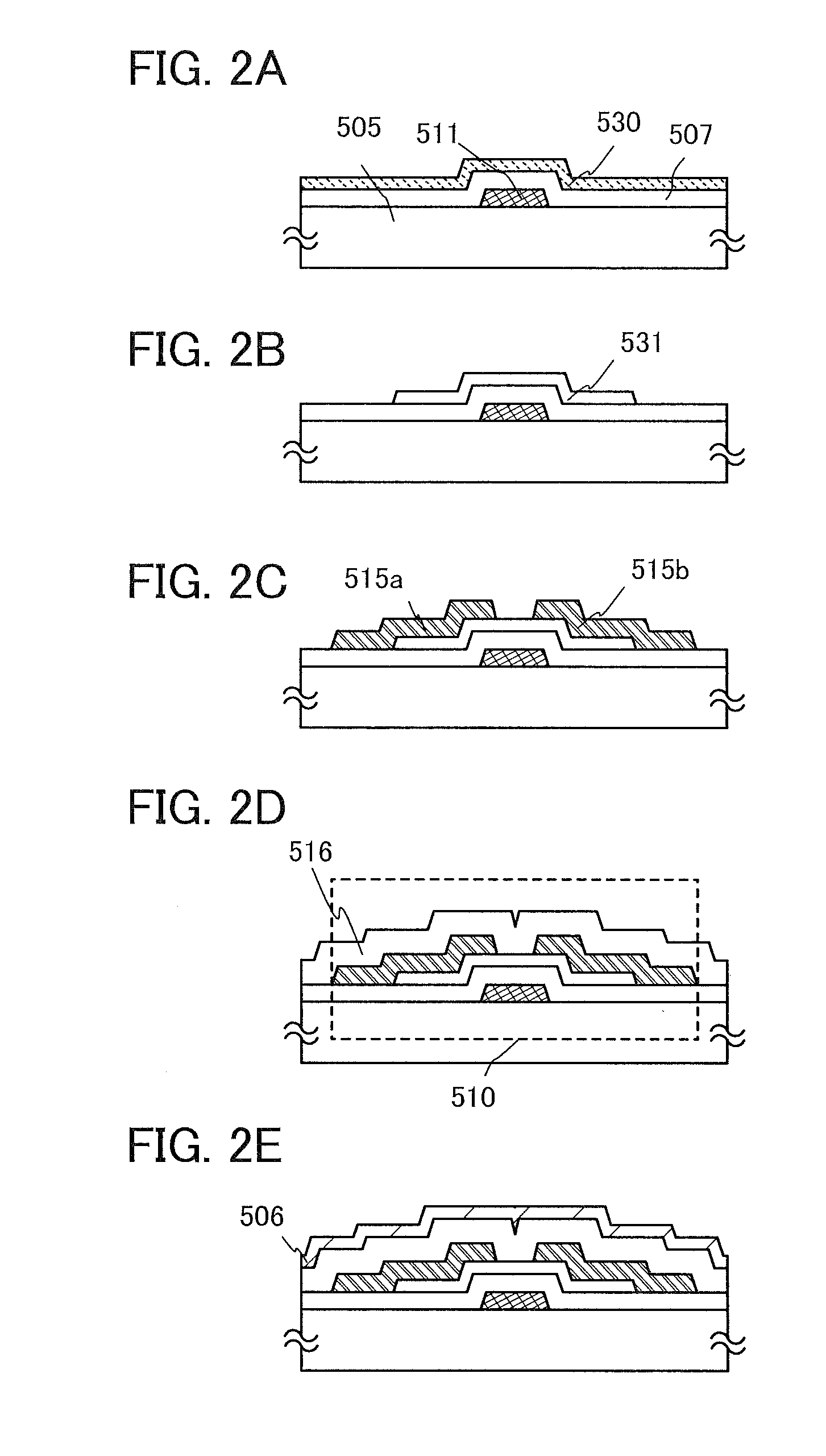
[0065]In this embodiment, examples of a structure of an inverted staggered transistor including an oxide semiconductor, a method for manufacturing the transistor and a method for designing a semiconductor device will be described with reference to FIGS. 2A to 2E and FIGS. 3A to 3D. Specifically, an enhancement transistor for design including an oxide semiconductor for design in a channel formation region is formed over an insulating surface of a substrate; an oxide insulating layer for design is formed so as to cover the transistor for design; an organic film for design is formed so as to cover the oxide insulating layer for design; a first electrode for design electrically connected to a source electrode layer or a drain electrode layer of the transistor for design is formed over the organic film for design; the first electrode for design is coated with deuterated water; a conductive film is formed in contact with the first electrode for design; a concentration of deuterium atoms i...
embodiment 3
[0160]In this embodiment, a structure of a light-emitting element in which an inert conductive material that reacts with deuterated water to a degree that does not easily allows generation of a deuterium ion or a deuterium molecule can be applied to a second electrode regardless of its work function will be described. Specifically, a structure of a light-emitting element in which an organic layer containing a light-emitting substance is provided between a first electrode which can be electrically connected to a source electrode layer or a drain electrode layer of an enhancement transistor including an oxide semiconductor in a channel formation region, and a second electrode; and a method for manufacturing the light-emitting element will be described with reference to FIG. 4.
[0161]Note that the structure of a light-emitting element exemplified in this embodiment can include a first electrode as an anode and a second electrode as a cathode. Alternatively, the first electrode can serve...
PUM
 Abstract
Description
Claims
Application Information