Method for Forming Lead-Free Solder Balls with a Stable Oxide Layer Based on a Plasma Process

a plasma process and oxide layer technology, applied in the direction of welding/cutting media/materials, soldering media, electrical equipment, etc., can solve the problems of less reliable connection, total contact failure, non-wet contact with the solder pad of the package substrate, etc., to achieve efficient passivation, avoid any elevated process temperature, and superior uniformity

Inactive Publication Date: 2012-03-01
GLOBALFOUNDRIES INC
View PDF3 Cites 4 Cited by
  • Summary
  • Abstract
  • Description
  • Claims
  • Application Information

AI Technical Summary

Benefits of technology

[0009]Generally, the present disclosure provides manufacturing techniques and strategies in which lead-free solder materials may be efficiently passivated by forming a passivation layer of well-controlled thickness and uniformity after the reflow process for forming the solder balls. To this end, a plasma-based process may be applied in order to treat any exposed surface areas of the solder balls, thereby avoiding any elevated process temperatures. In some illustrative embodiments disclosed herein, the plasma-based surface treatment may be performed on the basis of an oxygen plasma, which may result in the formation of an oxide layer of superior uniformity, wherein a thickness of the oxide layer may be determined on the basis of controlling at least one process parameter of the plasma treatment. In this manner, a wide variety of lead-free solder materials may be treated, such as solder materials containing tin and silver, solder materials containing tin and copper and the like, so that the resulting passivation layer may provide superior integrity during further manufacturing processes to be performed after the reflow process for forming the solder balls, while at the same time enabling an efficient removal of the passivation layer during the final solder process by using well-established flux materials.

Problems solved by technology

During the removal of the oxide layer by the flux material, however, any non-removed residuals of the oxide may significantly affect the solder process, which may result in a non-wet contact with the solder pad of the package substrate.
In this case, a less reliable connection or a total contact failure may result.
Consequently, the overall production yield in this very late manufacturing stage may significantly depend on the uniformity of the solder balls and thus on the uniformity and removability of the oxide layer formed thereon, since even a less reliable connection or the failure of a single solder ball may result in a total failure of the entire semiconductor device.
Moreover, lead material may also be a source of “soft” errors of the semiconductor device during operation, for instance by radioactive decay of non-stable isotopes, which may frequently be contained in the lead material.
Although the oxide layer may preserve integrity of the solder balls during the further processing, as is also discussed above, it turns out, however, that any non-uniformities of the oxide material may result in significant yield losses.
On the other hand, a well-controlled thermal re-oxidation process applied immediately after the reflow process, as described above, is difficult for the lead-free solder materials since the process temperature required for superior control of the thermal oxidation process is above the melting temperature of the lead-free solder material.

Method used


Image

  • Method for Forming Lead-Free Solder Balls with a Stable Oxide Layer Based on a Plasma Process
  • Method for Forming Lead-Free Solder Balls with a Stable Oxide Layer Based on a Plasma Process
  • Method for Forming Lead-Free Solder Balls with a Stable Oxide Layer Based on a Plasma Process

Examples


Embodiment Construction

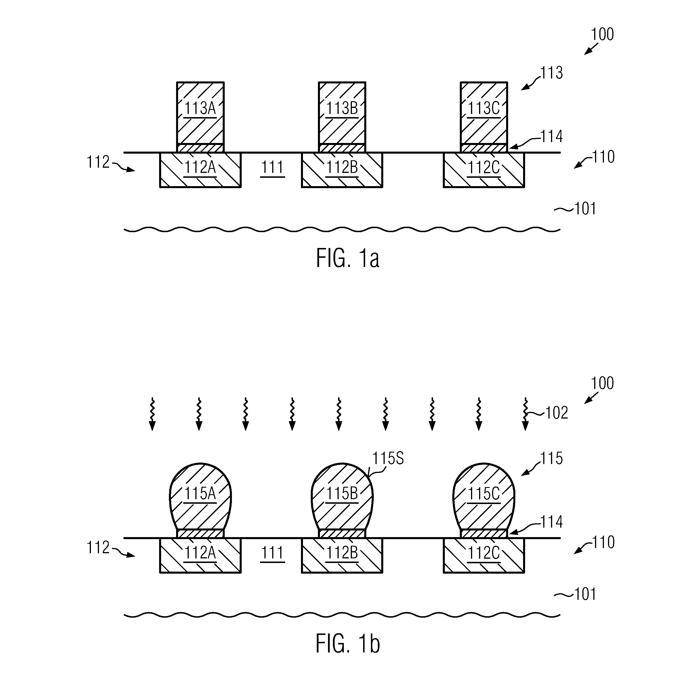
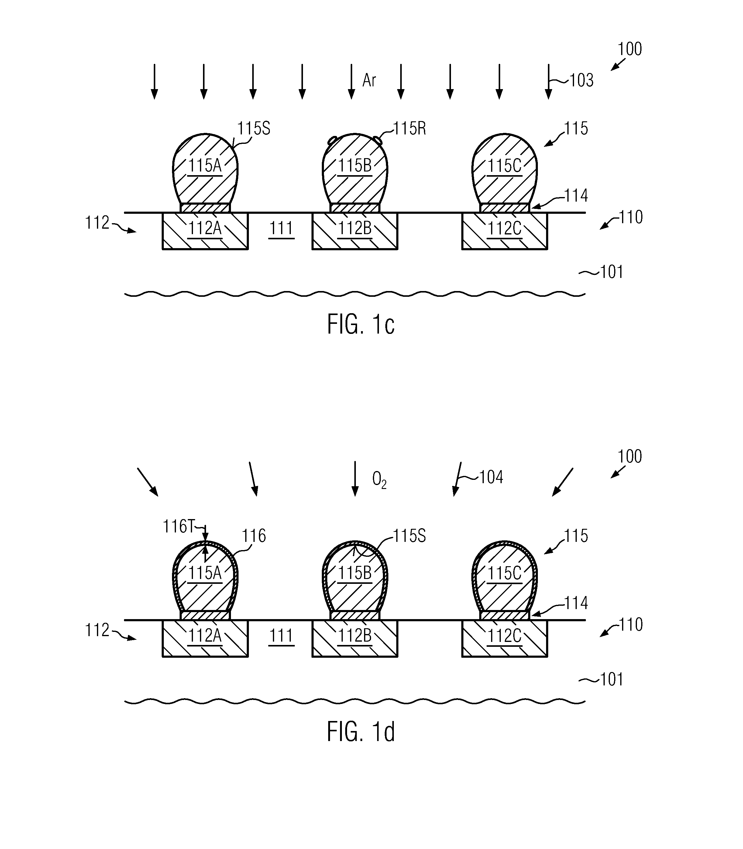
[0020]Various illustrative embodiments of the invention are described below. In the interest of clarity, not all features of an actual implementation are described in this specification. It will of course be appreciated that in the development of any such actual embodiment, numerous implementation-specific decisions must be made to achieve the developers' specific goals, such as compliance with system-related and business-related constraints, which will vary from one implementation to another. Moreover, it will be appreciated that such a development effort might be complex and time-consuming, but would nevertheless be a routine undertaking for those of ordinary skill in the art having the benefit of this disclosure.

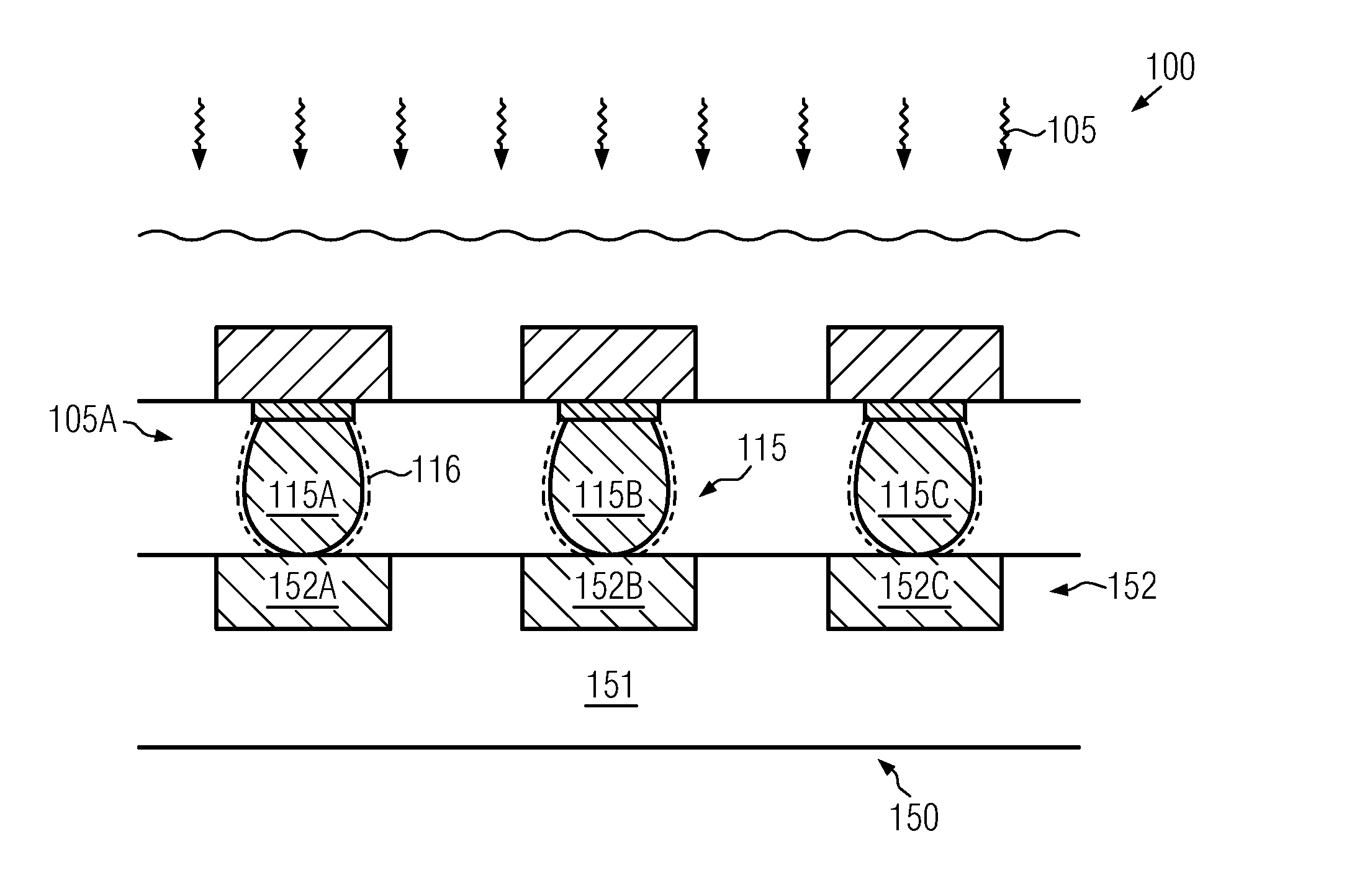
[0021]The present subject matter will now be described with reference to the attached figures. Various structures, systems and devices are schematically depicted in the drawings for purposes of explanation only and so as to not obscure the present disclosure with details ...


PUM

PropertyMeasurementUnit
thicknessaaaaaaaaaa
thicknessaaaaaaaaaa
timeaaaaaaaaaa

Abstract

Solder balls of semiconductor devices and, in particular, lead-free solder balls receive a very uniform passivation layer, for instance in the form of an oxide layer, which is formed by applying a plasma treatment. For example, the passivation layer may be provided with a thickness of 5-50 nm which may thus allow, due to the superior uniformity, a reliable protection of the solder balls while nevertheless ensuring a reliable removal during the final solder process.

Description

BACKGROUND OF THE INVENTION[0001]1. Field of the Invention[0002]The present disclosure generally relates to semiconductor devices comprising lead-free solder balls for directly attaching an appropriately formed package or carrier substrate to a die.[0003]2. Description of the Related Art[0004]In manufacturing integrated circuits, it is usually necessary to package a chip and provide leads and terminals for connecting the chip circuitry with the periphery. In some packaging techniques, chips, chip packages or other appropriate units may be connected by means of solder balls, formed from so-called solder bumps or bumps, which in turn are formed on metal regions of the metallization system of at least one of the units, for instance in the metallization system of the microelectronic chip. In order to connect the micro-electronic chip with the corresponding carrier, the surfaces of the two respective units to be connected, i.e., a microelectronic chip comprising, for instance, one or mor...

Claims


Application Information

Patent Timeline
Patent Type & Authority Applications(United States)
IPC IPC(8): H01L21/283
CPCB23K35/0244B23K35/262B23K35/3006B23K35/302B23K35/365B23K35/38B23K2201/40H01L24/11H01L2224/13099H01L2924/01013H01L2924/01029H01L2924/01047H01L2924/01082H01L2924/01327H01L2224/13687H01L2224/81011H01L24/13H01L24/81H01L2224/05647H01L2224/05655H01L2224/05666H01L2224/11462H01L2224/1147H01L2224/1181H01L2224/11849H01L2224/13111H01L2224/13562H01L2224/1357H01L2224/8181H01L2224/81815H01L2924/01005H01L2924/01006H01L2924/01033H01L2924/01068H01L2924/01074H01L2924/01075H01L2924/01322H01L2924/014H01L2224/1182H01L2924/00013H01L2224/0401H01L2924/1306H01L2924/00014H01L2224/13599H01L2224/05599H01L2224/05099H01L2224/29099H01L2224/29599H01L2924/00B23K2101/40H01L2924/14
Inventor ZENNER, SOERENJUNGNICKEL, GOTTHARDKUECHENMEISTER, FRANK
Owner GLOBALFOUNDRIES INC
Why Eureka
Try Eureka