N-type monocrystalline silicon HBC solar cell preparation method

A technology of solar cells and monocrystalline silicon, which is applied in the field of solar cells, can solve the problems of limiting the large-scale production of HBC cells, increasing the power generation per watt, and reducing LCOE, etc., and achieves the effects of low cost, simplified process, and simplified process steps

Inactive Publication Date: 2021-03-12
ZHEJIANG AIKO SOLAR ENERGY TECH CO LTD +2
View PDF5 Cites 1 Cited by
  • Summary
  • Abstract
  • Description
  • Claims
  • Application Information

AI Technical Summary

Problems solved by technology

However, due to the limitations of its technical mechanism, the P-type PERC cell has encountered a bottleneck in improving the conversion efficiency. The N-type HBC cell combines the advantages of full light receiving of the back contact cell and high-quality passivation of the heterojunction cell, and its experimental efficiency reaches 26.63%. , the efficiency is greatly im

Method used


Image

  • N-type monocrystalline silicon HBC solar cell preparation method
  • N-type monocrystalline silicon HBC solar cell preparation method
  • N-type monocrystalline silicon HBC solar cell preparation method

Examples


Example Embodiment

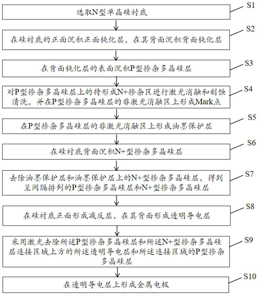
[0048] See figure 1 The present invention provides an N-type single crystal silicon HBC solar cell preparation method, including:

[0049] S1, select the n-type single crystal silicon substrate 1;

[0050] As the preferred embodiment, including:

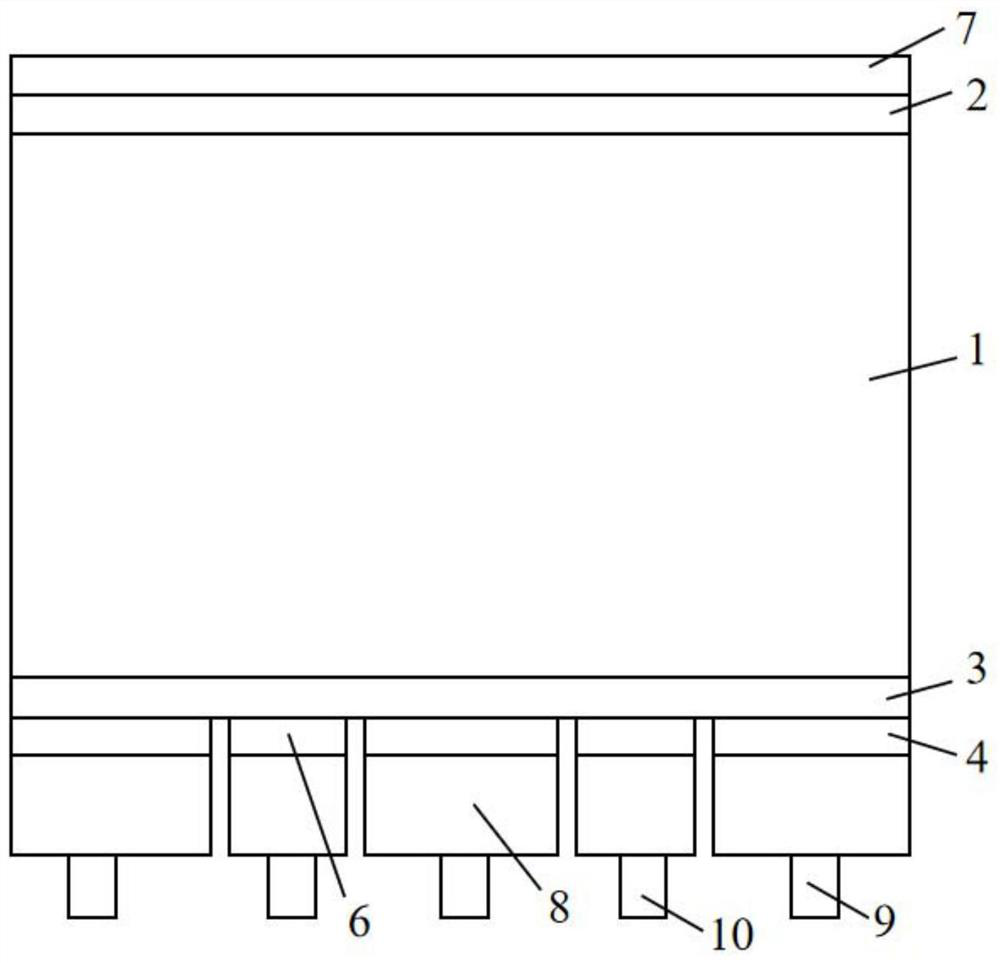
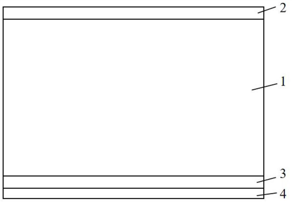
[0051] Select the back polishing, the front surface of the n-type single crystal silicon substrate 1 is provided; the resistivity of the N-type single crystal silicon substrate 1 is from 1 to 15 Ω · cm, and the thickness is 60-250 μm.

[0052] S2, the front passivation layer 2 is deposited on the front side of the silicon substrate 1, and the back surface passivation layer 3 is deposited thereof;

[0053] As a preferred embodiment, including:

[0054] The front pass passivation layer 2 and the back passivation layer 3 are deposited in the front and back surfaces of the n-type single crystal silicon substrate 1 by the LPCVD device.

[0055] The front passivation layer 2 and the back passivation layer 3 are made of one or more of silicon o...

Example Embodiment

[0106] Example 1

[0107] Method for preparing n-type single crystal silicon HBC solar cell, including:

[0108] S1, select the back surface polishing, the front surface of the N-type single crystal silicon substrate, the N-type single crystal silicon substrate is 15 Ω · cm, and the thickness is 250 μm;

[0109] S2, the front pass passivation layer and the back surface passivation layer are deposited on the surface of the silicon substrate using the LPCVD device; the thickness of the front passivation layer and the back passivation layer is 20 nm;

[0110] S3, using the LPCVD device to deposit the P-type doped polysilicon layer on the surface of the back passivation layer; the P-type doped polysilicon layer is a composite film of 5 layers, each layer thickness of 30 nm, and the total thickness is 150 nm; the P-type The doping concentration of the doped polysilicon layer is incremented by the intrinsic layer interface to the conductive layer interface, and the boron doped concentra...

Example Embodiment

[0118] Example 2

[0119] Method for preparing n-type single crystal silicon HBC solar cell, including:

[0120] S1, select the back polishing, the front of the N-type single crystal silicon substrate is provided, the resistivity of the n-type single crystal silicon substrate is 5 Ω · cm, and the thickness is 60 μm;

[0121] S2, using the LPCVD device to deposit a front passivation layer and a back passivation layer on the surface of the silicon substrate; the thickness of the front passivation layer and the back passivation layer is 5 nm;

[0122] S3, using the LPCVD device to deposit the P-type doped polysilicon layer on the surface of the back passivation layer; the P-type doped polysilicon layer is a two-layer composite film having a thickness of 50 nm, a total thickness of 100 nm; the P-type The doping concentration of the doped polysilicon layer is sequentially incremented by the intrinsic layer interface to the conductive layer interface, and the boron doped concentration r...


PUM

PropertyMeasurementUnit
Thicknessaaaaaaaaaa
Wavelengthaaaaaaaaaa
Diameteraaaaaaaaaa

Abstract

The invention discloses an N-type monocrystalline silicon HBC solar cell preparation method, and the method comprises the steps: employing LPCVD equipment and Mark point positioning technology, employing a laser ablation technology to cooperate with an ink protection layer to prepare a P-type doped polycrystalline silicon layer and an N+type doped polycrystalline silicon layer which are arranged at intervals in an interdigital manner, and obtaining an HBC cell with better passivation, higher open-circuit voltage, higher efficiency and lower cost. By adopting the method, the preparation methodof the N-type monocrystalline silicon HBC solar cell is simplified, the N-type monocrystalline silicon HBC solar cell which is good in passivation effect, high in starting voltage and high in efficiency is obtained, and the simple-process, low-cost and high-efficiency large-scale production of the N-type monocrystalline silicon HBC solar cell is realized.

Description

Technical field [0001] The present invention relates to the field of solar cell technology, and more particularly to an N-type single crystal silicon HBC solar cell preparation method. Background technique [0002] In recent years, the application of p-type PERC battery technology has increased solar cell conversion efficiency from 20% to 22.50%, and the battery cost is reduced from 3.0 yuan / w to 0.80 yuan / W, and PERC batteries have become the largest battery share. At the same time, Power generation costs enter a parity era. However, PERC batteries are limited by its technical mechanism, and the current improvement conversion efficiency has encountered bottlenecks, N-type HBC batteries combined with back contact with battery full light and heterogeneous batteries. High quality passivation, its experimental efficiency reached 26.63% The significant increase in efficiency is increased. On the one hand, the battery itself is increased, and the other aspect is advantageous to re...

Claims


Application Information

Patent Timeline
IPC IPC(8): H01L31/18H01L31/068H01L31/0463H01L31/0216H01L23/544
CPCH01L31/1804H01L31/1868H01L31/0682H01L31/0463H01L23/544H01L31/02167H01L31/02168Y02E10/546Y02P70/50Y02E10/547
Inventor 田得雨林纲正陈刚
Owner ZHEJIANG AIKO SOLAR ENERGY TECH CO LTD
Why Eureka
Try Eureka