Supercharge Your Innovation With Domain-Expert AI Agents!

Semiconductor device

a semiconductor device and semiconductor technology, applied in semiconductor devices, digital storage, instruments, etc., can solve the problems of data not being written and read correctly, the size and cost of a semiconductor device are increased, and the number of required circuits is increased, so as to reduce the effect of variation in the transistor of a memory cell and increase the writing potential. , the effect of reading curren

Active Publication Date: 2012-03-15
SEMICON ENERGY LAB CO LTD
View PDF5 Cites 24 Cited by
  • Summary
  • Abstract
  • Description
  • Claims
  • Application Information

AI Technical Summary

Benefits of technology

[0013]However, in a multilevel memory, a variety of different potential values are used along with a mass storage; therefore, there are problems in that the number of required circuits is increased and the size and cost of a semiconductor device are increased.

Problems solved by technology

However, in a multilevel memory, a variety of different potential values are used along with a mass storage; therefore, there are problems in that the number of required circuits is increased and the size and cost of a semiconductor device are increased.
Because of these variations, there is a problem in that data cannot be written and cannot be read correctly in some cases.
In other words, when judgment is performed in such a state, the potential in reading of data is below the threshold potential due to discharge of a little charge, so that wrong data is read.
When a phenomenon in which the threshold potential varies due to noise or the like from the outside, a so-called chattering phenomenon occurs, there is a problem in that reading of data cannot be performed correctly.
However, these methods have a problem in that a circuit size is increased and power consumption is also increased.

Method used


Image

  • Semiconductor device
  • Semiconductor device
  • Semiconductor device

Examples


embodiment 1

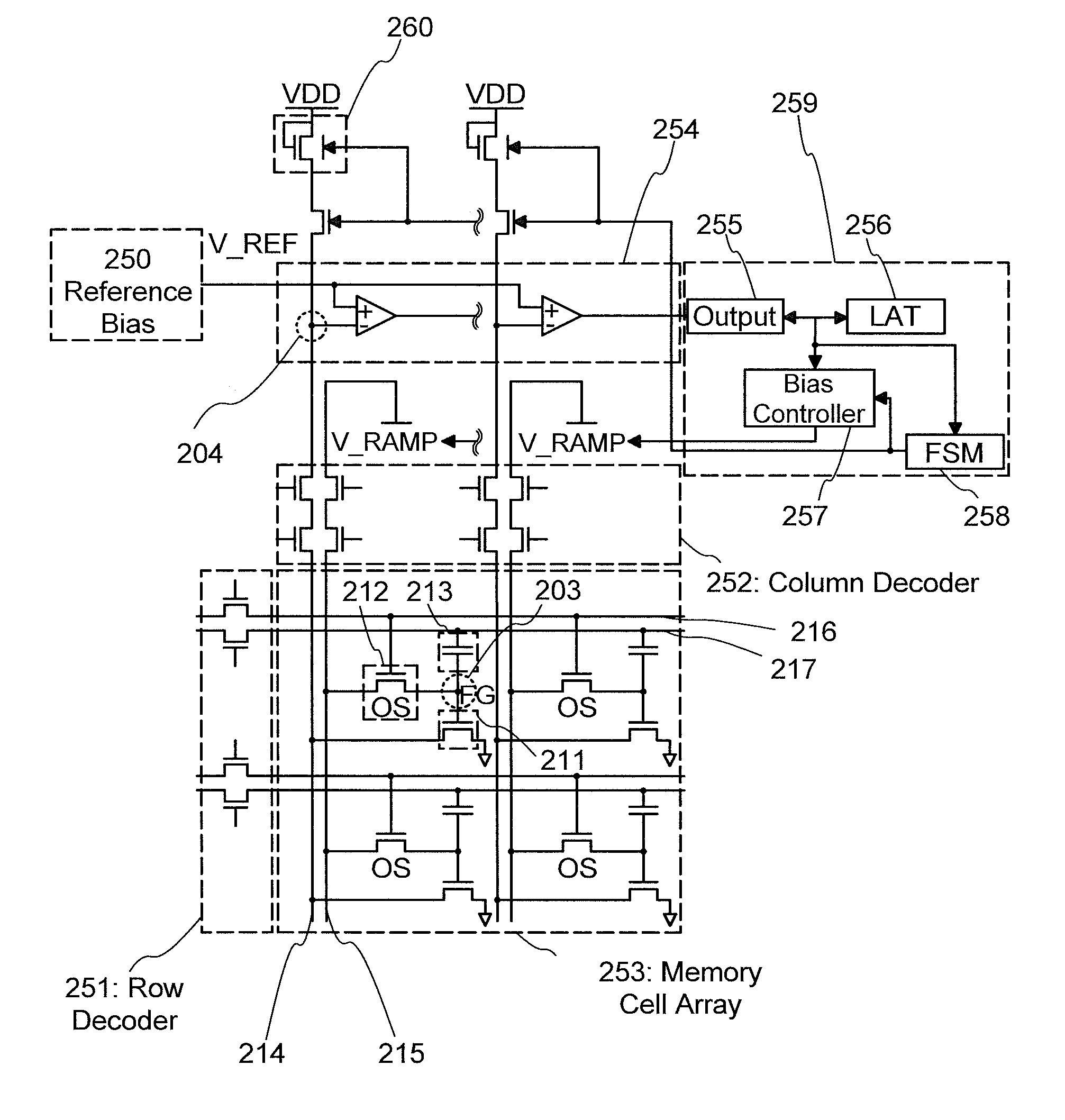
[0058]In this embodiment, a semiconductor device according to one embodiment of the invention disclosed herein will be described with reference to FIG. 1, FIG. 2, and FIGS. 3A and 3B. Note that in some circuit diagrams, “OS” is written beside a transistor in order to indicate that the transistor includes an oxide semiconductor (OS).

[0059]First, a circuit configuration will be described with reference to FIG. 1. The circuit configuration in FIG. 1 is a NOR memory (1 bit / cell) and includes a memory cell array 253 in which a plurality of memory cells is arranged in a matrix, a reference potential circuit 250, a potential comparison circuit 254, a control circuit 259 used for controlling the driving, and a resistor 260 including a transistor.

[0060]The circuit configuration may be provided with a peripheral circuit such as a word line selection circuit 251 (Row Decoder) or a bit line selection circuit 252 (Column Decoder), as appropriate.

[0061]The memory cell array 253 includes a first t...

embodiment 2

[0105]Next, a circuit configuration which is different from the circuit configuration illustrated in FIG. 1 and a driving method thereof will be described with reference to FIG. 4, FIGS. 5A and 5B, FIGS. 6A and 6B, FIGS. 7A and 7B, and FIGS. 8A and 8B.

application example

[0106]A difference between FIG. 1 and FIG. 4 is that the circuit configuration illustrated in FIG. 1 is the 1 bit / cell whereas the circuit configuration illustrated in FIG. 4 is a multilevel memory circuit of a 2 bit / cell.

[0107]The multilevel memory circuit in FIG. 4 includes a reference potential circuit 350 (Reference Bias 1) which transmits a signal of a reference potential, a reference potential circuit 360 (Reference Bias 2), a reference potential circuit 370 (Reference Bias 3), a word line selection circuit 351 (Row Decoder) which selects / controls an address of a word line, a bit line selection circuit 352 (Column Decoder) which selects / controls an address of a bit line, a memory cell array 353 which stores data, a potential comparison circuit 354a which compares a reference potential output from the reference potential circuit 350 and a potential of the memory cell array 353, a potential comparison circuit 354b which compares a reference potential output from the reference po...


PUM


Abstract

One object is to provide a novel semiconductor device which can hold stored data even when not powered and which has an unlimited number of writing operations. Another object is to reduce a circuit size and to improve reliability of writing and reading of data. When a memory cell using a transistor including an oxide semiconductor layer is subjected to the verification operation and reading of data, a dual-gate transistor showing different threshold voltages is used as a resistor; thus, stable verification operation and reading operation can be performed by only a reference potential circuit.

Description

BACKGROUND OF THE INVENTION[0001]1. Field of the Invention[0002]One embodiment of the invention disclosed herein relates to a semiconductor device including a semiconductor element.[0003]2. Description of the Related Art[0004]Memory devices including semiconductor elements, which are included in the category of semiconductor devices, are broadly classified into two categories: volatile memory devices that lose stored data when not powered, and nonvolatile memory devices that hold stored data even when not powered.[0005]A typical example of volatile memory devices is a dynamic random access memory (DRAM). A DRAM stores data in such a manner that a transistor included in a storage element is selected and charge is held in a capacitor.[0006]When data is read from a DRAM, charge in a capacitor is lost according to the above-described principle; thus, another writing operation is necessary every time data is read out. Moreover, a transistor included in a memory element has leakage curren...

Claims


Application Information

Patent Timeline
IPC IPC(8): G11C11/24
CPCG11C16/0466H01L27/1225H01L27/1207H01L27/11517H10B41/00
Inventor KAMATA, KOICHIRO
Owner SEMICON ENERGY LAB CO LTD
Features
  • R&D
  • Intellectual Property
  • Life Sciences
  • Materials
  • Tech Scout
  • Unparalleled Data Quality
  • Higher Quality Content
  • 60% Fewer Hallucinations
Learn More