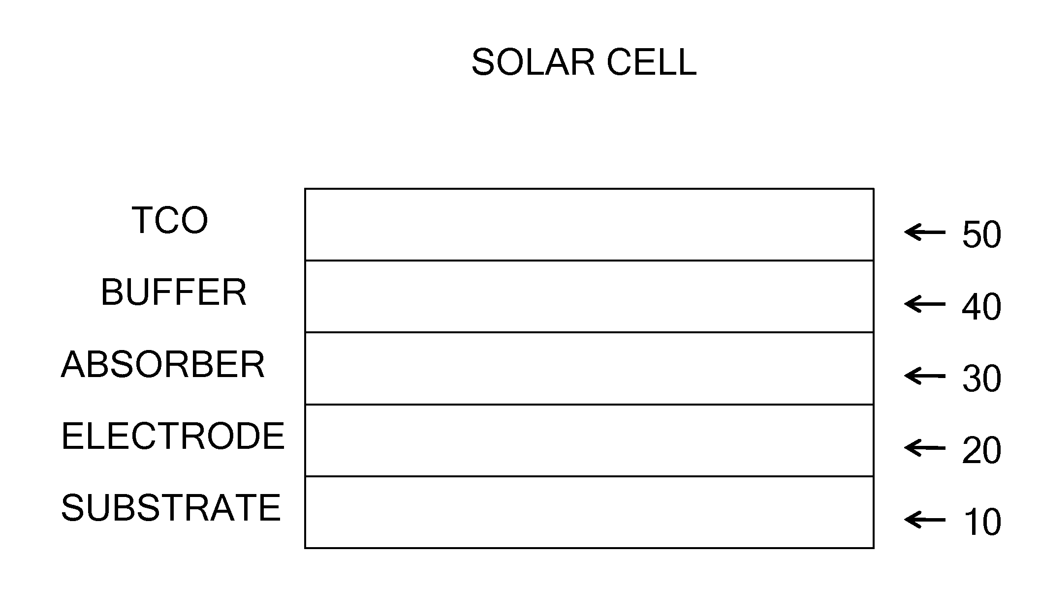
Deposition processes and photovoltaic devices with polymeric precursors
- Summary
- Abstract
- Description
- Claims
- Application Information
AI Technical Summary
Benefits of technology
Problems solved by technology
Method used
Image

Examples
example 1
[0613]A solar cell was made by the following process.
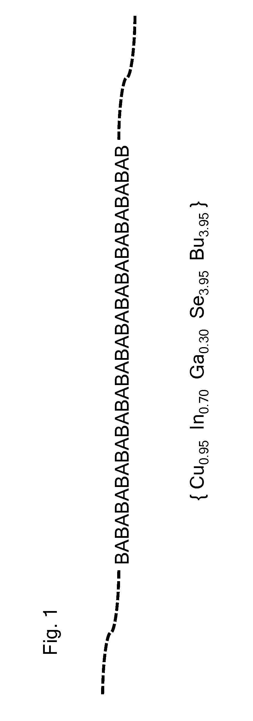
[0614]A first ink was prepared by dissolving the Cu-enriched CIGS polymeric precursor compound {Cu1.1In0.7Ga0.3(SetBu)1.1(SenBu)3.0} with 0.5 at % Na supplied via NaIn(SenBu)4 in heptane, 50% polymeric precursor content, by weight, followed by dilution with cyclohexane to about 25% polymeric precursor content, by weight, in an inert atmosphere glove box. The resulting ink was filtered through a 0.2 μm PTFE syringe filter prior to use.
[0615]A second ink was made prepared by dissolving the Cu-deficient CIGS polymeric precursor compound {Cu0.85In0.7Ga0.3(SetBu)0.85(SenBu)3.0} with 0.5 at % Na supplied via NaIn(SenBu)4 in heptane, 25% polymeric precursor content, by weight, in an inert atmosphere glove box. The resulting ink was filtered through a 0.2 μm PTFE syringe filter prior to use.
[0616]An 0.04 mL aliquot of the first ink was deposited onto a piece of 2 inch by 2 inch square Mo-coated sodalime glass substrate using a knife coate...
example 2
[0624]A solar cell was made by the following process.
[0625]A first ink was prepared by dissolving the Cu-enriched CIGS polymeric precursor compound {Cu1.1In0.7Ga0.3(SetBu)1.1(SenBu]3.0} with 0.5 at % Na supplied via NaIn(SenBu)4 in heptane, 50% polymer content, by weight, followed by dilution with cyclohexane to about 25% polymer content, by weight, in an inert atmosphere glove box. The resulting ink was filtered through a 0.2 μm PTFE syringe filter prior to use.
[0626]A second ink was made prepared by dissolving the Cu-deficient CIGS polymeric precursor compound {Cu0.85In0.7Ga0.3(SetBu)0.85(SenBu)3.0} with 0.5 at % Na supplied via NaIn(SenBu)4 in heptane, 25% polymer content, by weight, in an inert atmosphere glove box. The resulting ink was filtered through a 0.2 μm PTFE syringe filter prior to use.
[0627]An 0.04 mL aliquot of the first ink was deposited onto a piece of 2 inch by 2 inch square Mo-coated sodalime glass substrate using a knife coater (Global Instrument) in an inert ni...
example 3
[0630]A solar cell was made by the following process.
[0631]A first ink was prepared by dissolving {Cu1.1In0.7Ga0.3(SetBu)1.1(SenBu]3.0} with 0.5 at % Na supplied via NaIn(SenBu)4 in heptane, 25% polymer content, by weight, in an inert atmosphere glove box. The resulting ink was filtered through a 0.2 μm PTFE syringe filter prior to use.
[0632]A second ink was made prepared by dissolving {Cu0.85In0.7Ga0.3(SetBu)0.85(SenBu)3.0} with 0.5 at % Na supplied via NaIn(SenBu)4 in heptane, 25% polymer content, by weight, in an inert atmosphere glove box. The resulting ink was filtered through a 0.2 μm PTFE syringe filter prior to use.
[0633]An 0.04 mL aliquot of the first ink was deposited onto a piece of 2 inch by 2 inch square Mo-coated sodalime glass substrate using a knife coater (RK Instruments) in an inert nitrogen atmosphere glove box with a knife speed of 20 mm / s The wet polymer film on the substrate was transferred to a pre-heated 300° C. hot plate for 5 minutes to dry and convert the ...
PUM
 Abstract
Description
Claims
Application Information
 - Generate Ideas
- Intellectual Property
- Life Sciences
- Materials
- Tech Scout
- Unparalleled Data Quality
- Higher Quality Content
- 60% Fewer Hallucinations
Browse by: Latest US Patents, China's latest patents, Technical Efficacy Thesaurus, Application Domain, Technology Topic, Popular Technical Reports.
© 2025 PatSnap. All rights reserved.Legal|Privacy policy|Modern Slavery Act Transparency Statement|Sitemap|About US| Contact US: help@patsnap.com