Conducting paste for device level interconnects

a technology of conducting paste and interconnects, which is applied in the direction of conductors, non-metal conductors, printed circuit non-printed electric components association, etc., can solve the problems of no mechanical strength of high loading systems and no prior art disclosure of creating conducting pastes for interconnects

Inactive Publication Date: 2012-03-22
TTM TECH NORTH AMERICA LLC
View PDF4 Cites 8 Cited by
  • Summary
  • Abstract
  • Description
  • Claims
  • Application Information

AI Technical Summary

Benefits of technology

[0011]A conducting paste with metal loading in the range of 80-95% is obtained by mixing two different conducting pastes, in which each paste maintains its micro level individual rich region in the mixed paste even after final curing. One paste contains at least one low melting point alloy and the other paste contains noble metal fillers such as gold or silver flakes. Generally, the process is performed by embedding nano particles within a polymer constituent. Next, the polymer and nano particles are dissolved in an organic solvent which prevents sintering of the nano particles in the presence of the polymers.

Problems solved by technology

Historically, this junction of the connections between five micron device level interconnects, such as the sensor and the processor, has created a problem.
Current commercially available paste makes it necessary to load a higher metal for sintering in these pastes, but a high loading system has no mechanical strength.
The existing prior art tends to deal with conducting paste that has the same problems as the commercially available paste listed above.
None of the prior art discloses creating a conducting paste for interconnects that includes the same materials and method to connect micron interconnects such as sensors or chips.
In addition, the paste is not made by mixing two different conducting pastes, where each paste maintains its own micro level individual rich region in the mixed paste even after final curing.

Method used


Image

  • Conducting paste for device level interconnects
  • Conducting paste for device level interconnects
  • Conducting paste for device level interconnects

Examples


Embodiment Construction

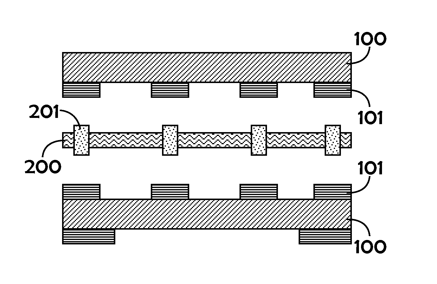
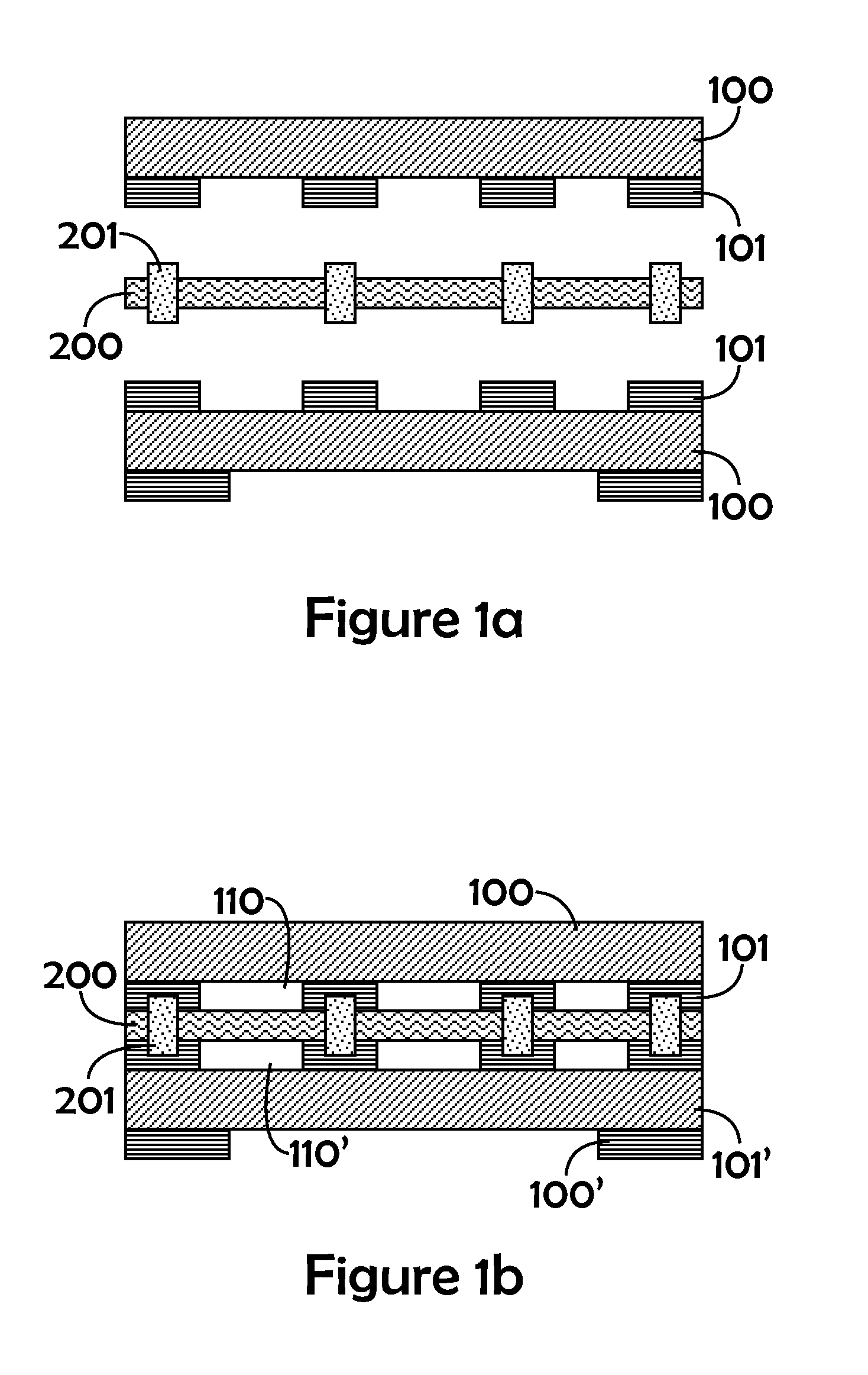
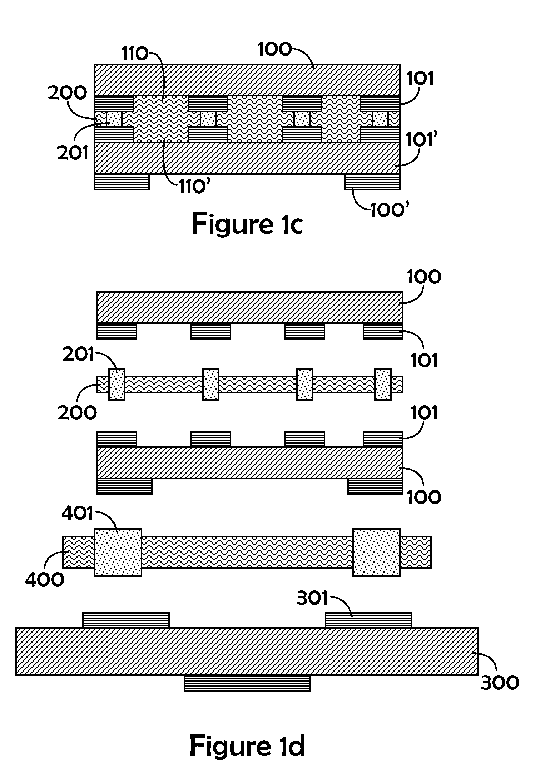
[0030]For a better understanding of the present invention, together with other and further objects, advantages, and capabilities thereof, reference is made to the following disclosure and appended claims in connection with the above-described drawings. The present invention is further described with reference to the accompanying figures where like reference numbers correspond to the same elements.

[0031]An example of an embodiment of this invention is a nano-micro conducting paste made using fifty grams of cycloaliphatic epoxy resin (e.g., one sold under product designation “ERL-4211” by the Union Carbide Corporation, Danbury, Conn.) mixed with about 50 g of hexahydro-4-methylphthalic anhydride and 0.4 g N, N dimethyl benzylamine. Further, 5 g of silver nano particles with average particle size 10-15 nanometers and 6 g of silver micro particles with average particle size five microns is thoroughly added to the mixtures. Then, 11 g of mixed silver is added to 2.5 g of the cycloaliphat...


PUM

PropertyMeasurementUnit
sizeaaaaaaaaaa
temperaturesaaaaaaaaaa
sizeaaaaaaaaaa

Abstract

A conducting paste and method of forming the paste for device level interconnection. The conducting paste contains metal loading in the range 80-95% that is useful for making five micron device level interconnects. The conducting paste is made by mixing two different conducting pastes, each paste maintaining its micro level individual rich region in the mixed paste even after final curing. One paste contains at least one low melting point alloy and the other paste contains noble metal fillers such as gold or silver flakes. In general, average flake size below five micron is suitable for five micron interconnects. However, 1 micron or smaller silver flakes and an LMP mixture is preferred for five micron interconnects. The amount of LMP based paste in the final mixture is preferably 20-50% by weight. The nano micro paste embodiment shows good electrical yield (81%) and low contact resistance.

Description

FIELD OF INVENTION[0001]The present invention relates to electrically conducting paste for device level interconnects and methods of making same and, more specifically, to conducting paste that can be used for connecting micron interconnects, such as sensors or chips, for devices such as infrared (IR) camera systems.BACKGROUND OF THE INVENTION[0002]One of the steps of sensor fabrication when developing device systems such as are used for infrared (IR) cameras involves the use of a conducting paste to make connections between interconnects of the device. Historically, this junction of the connections between five micron device level interconnects, such as the sensor and the processor, has created a problem. Current commercially available paste makes it necessary to load a higher metal for sintering in these pastes, but a high loading system has no mechanical strength. However, even when a low metal loading system is used, no sintering occurs even at very high temperatures (e.g., 300°...

Claims


Application Information

Patent Timeline
Patent Type & Authority Applications(United States)
IPC IPC(8): H05K7/00H01B1/02H01B1/22H01R43/00
CPCY10T29/49117H01B1/22H01L2224/81
Inventor DAS, RABINDRA N.MAGNUSON, ROY H.POLIKS, MARK D.MARKOVICH, VOYA R.
Owner TTM TECH NORTH AMERICA LLC
Why Eureka
Try Eureka