
High volume method of making low-cost, lightweight solar materials

Inactive Publication Date: 2012-03-29
UT BATTELLE LLC
View PDF71 Cites 18 Cited by
  • Summary
  • Abstract
  • Description
  • Claims
  • Application Information

AI Technical Summary

Benefits of technology

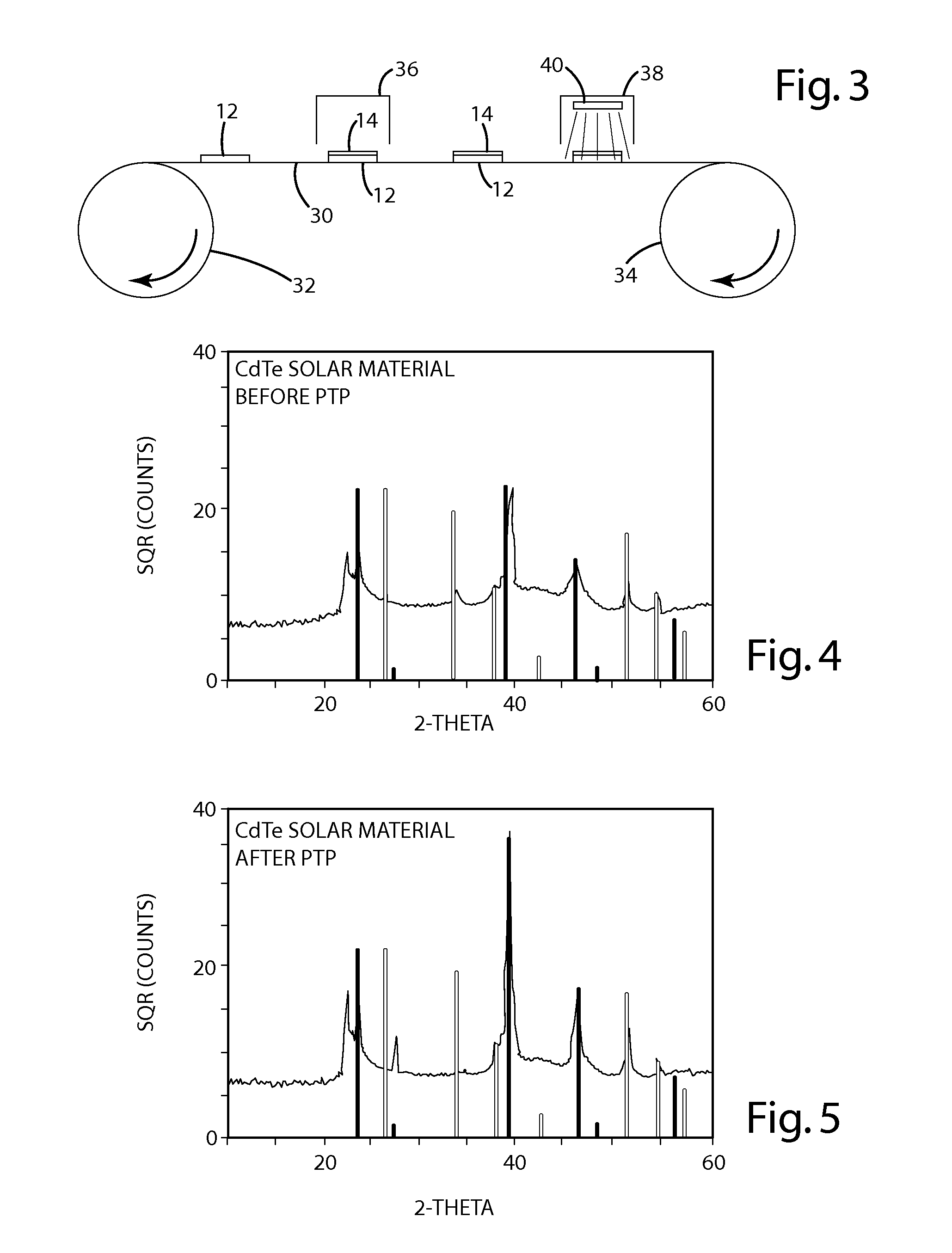
[0008]According to a second aspect of the present invention, a method of manufacturing a photovoltaic device includes exposing a photovoltaic precursor to energy of a sufficient intensity and for sufficient duration to convert the precursor into a crystalline photovoltaic material without materially affecting an underlying substrate. In particular, the method can include directing one or more intense pulses of radiant energy toward a superficial region of the photovoltaic precursor opposite the substrate without causing the substrate to exceed its upper operating temperature, thereby achieving a grain growth and an increased photovoltaic efficiency.
[0010]The present invention provides an effective photovoltaic device and method for fabricating a photovoltaic device on a substrate having a relatively low upper operating temperature. The method of the present invention is relatively inexpensive and permits the use of polymeric substrates that might otherwise be damaged by energy or heat from conventional methods. In addition, the use of polymeric substrates can greatly reduce the weight of the photovoltaic device and can eliminate the cost and complexity of prior art methods of crystallizing photovoltaic precursors. Combining the pulsed thermal processing of the present invention with high volume deposition techniques can result in moderately efficient solar cells with greater than 5% efficiency at extremely low manufacturing costs (˜$0.30 / W).

Problems solved by technology

Many polymer substrates have an upper operating temperature (i.e., the temperature at which the material will degrade or decompose) well below 400° C., while most photovoltaic precursors are processed according to conventional methods at temperatures in excess of 600° C. As a result, low cost manufacturing approaches such as roll-to-roll techniques are often not permitted due to the high temperature processing required of most photovoltaic precursors.
Even where the solar cell includes a thermally-insulating layer between the substrate and the photovoltaic precursor, conventional heating methods can damage both the substrate and the substrate-precursor interface.
In the absence of an annealing step, however, the resulting efficiencies can be poor.

Method used


Image

  • High volume method of making low-cost, lightweight solar materials
  • High volume method of making low-cost, lightweight solar materials
  • High volume method of making low-cost, lightweight solar materials

Examples


Embodiment Construction

[0022]The invention as contemplated and disclosed herein can greatly improve the manufacture and processing of high efficiency photovoltaics. In particular, the present invention includes a process using intense pulses of radiant energy to improve the material quality and grain size of photovoltaic precursor(s) supported by a flexible substrate.

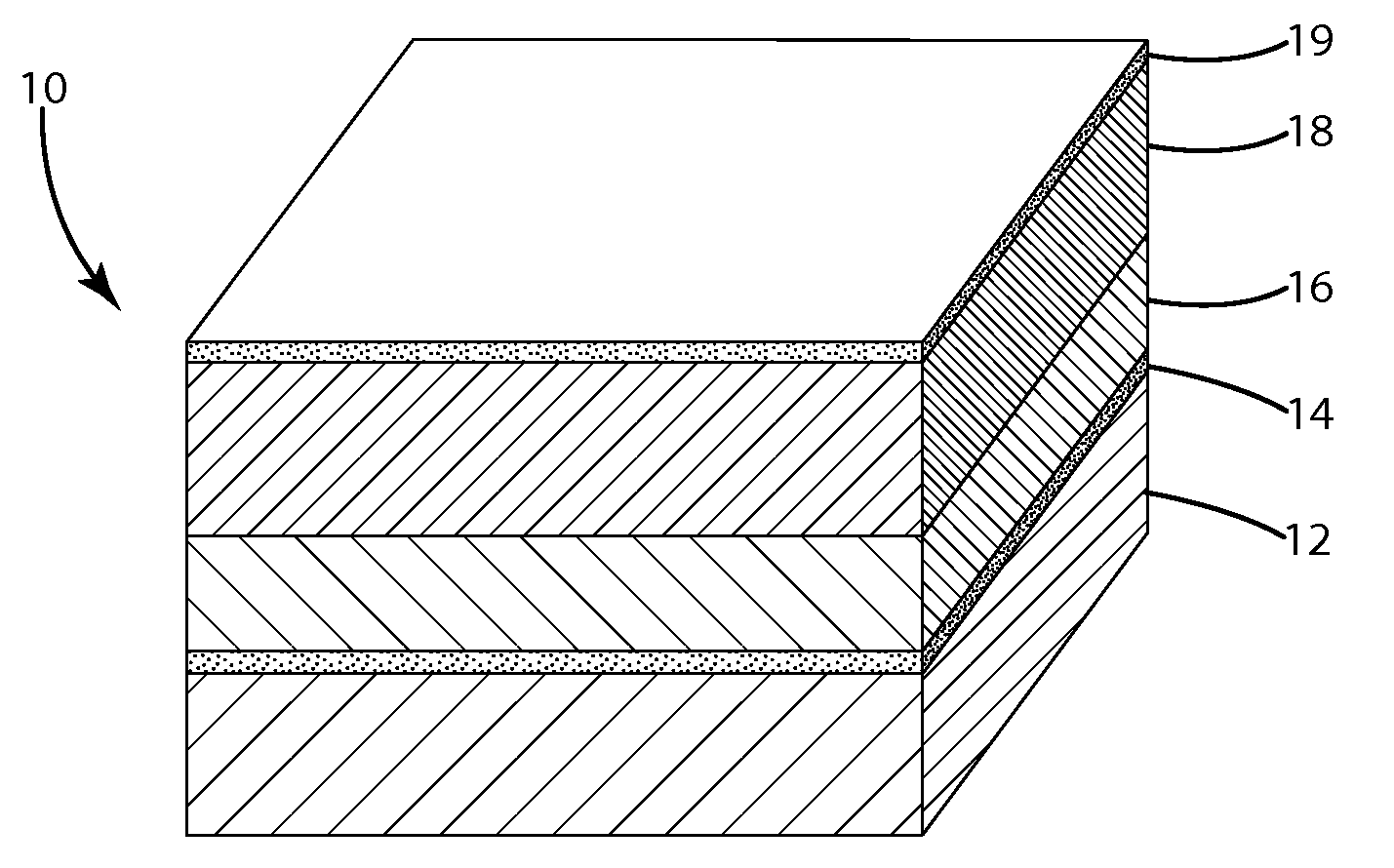
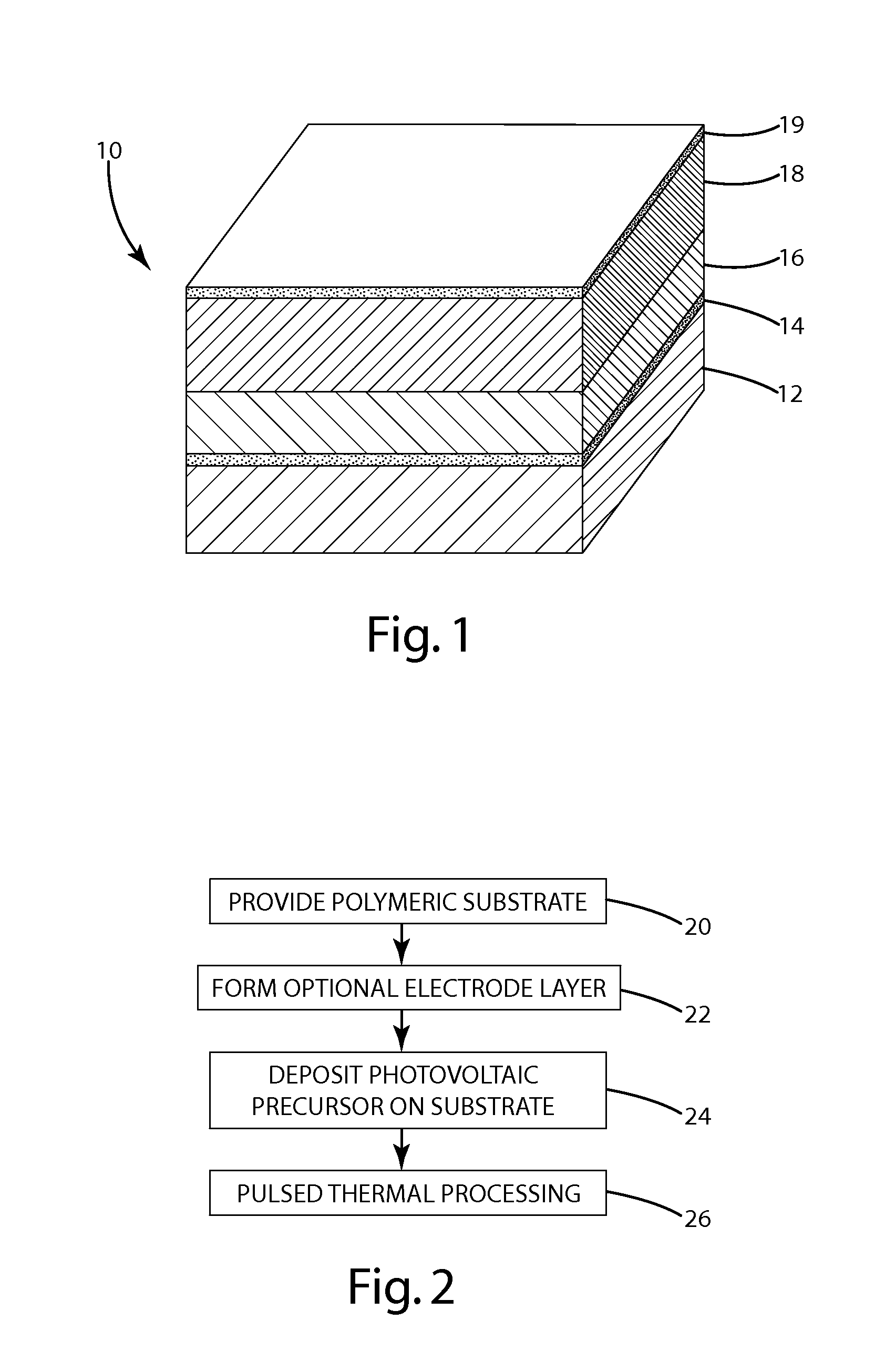
[0023]FIG. 1 shows a partial cross-section of one example of a photovoltaic device 10 manufactured in accordance with the present invention. The photovoltaic device 10 can form part of a solid-state semiconductor solar cell or any other photovoltaic cell adapted to convert solar energy into electricity. The photovoltaic device 10 may be fabricated in sheets of a size appropriate for its intended use. It may also be fabricated on small substrates or in configurations other than sheets. For example, the photovoltaic device 10 may be fabricated as a small solar cell for a hand-held electronic device or on large sheets to be applied to large area...


PUM


Abstract

A thin film solar cell and a method fabricating thin film solar cells on flexible substrates. The method includes including providing a flexible polymeric substrate, depositing a photovoltaic precursor on a surface of the substrate, such as CdTe, ZrTe, CdZnTe, CdSe or Cu(In,Ga)Se2, and exposing the photovoltaic precursor to at least one 0.5 microsecond to 10 second pulse of predominately infrared light emitted from a light source having a power output of about 20,000 W / cm2 or less to thermally convert the precursor into a crystalline photovoltaic material having a photovoltaic efficiency of greater than one percent, the conversion being carried out without substantial damage to the substrate.

Description

[0001]This invention was made with government support under Contract No. DE-AC05-00OR22725 awarded by the U.S. Department of Energy. The government has certain rights in the invention.BACKGROUND OF THE INVENTION[0002]The present invention relates to a method for fabricating solar cells, and more particularly, a method for fabricating solar cells on flexible substrates.[0003]The conversion of light into electricity occurs over a wide variety of photovoltaic materials. For example, photovoltaic materials include single element semiconductors, such as amorphous silicon and thin-film crystalline silicon, as well as compound semiconductors, such as cadmium telluride (CdTe) and copper indium gallium (di)selenide (Cu(In,Ga)Se2 or CIGS). These and other photovoltaic materials absorb photons of energy sufficient to create electron-hole pairs across a junction, thereby creating an internal electric field. The internal electric field results in a buildup of voltage between two electrodes to pr...

Claims


Application Information

Patent Timeline
IPC IPC(8): H01L31/0336H01L31/18
CPCH01L31/0296H01L31/02966H01L31/03925Y02E10/543H01L31/1832H01L31/1836H01L31/1828Y02P70/50
Inventor BLUE, CRAIG A.CLEMONS, ARTDUTY, CHAD E.HARPER, DAVID C.OTT, RONALD D.RIVARD, JOHN D.
Owner UT BATTELLE LLC
Learn More