Heat treatment apparatus and heat treatment method for heating substrate by irradiating substrate with flashes of light

a heat treatment apparatus and substrate technology, applied in the direction of optical radiation measurement, muffle furnace, furnace, etc., can solve the problems of poor device formation, inability to make real-time measurements of the surface temperature of the substrate, and large junction depth

Active Publication Date: 2012-03-29
DAINIPPON SCREEN MTG CO LTD
View PDF21 Cites 18 Cited by
  • Summary
  • Abstract
  • Description
  • Claims
  • Application Information

AI Technical Summary

Benefits of technology

[0014]This prevents the flashes of light emitted from the xenon flash lamp from serving as disturbance light.
[0019]This prevents the flashes of light emitted from the xenon flash lamp from serving as disturbance light.

Problems solved by technology

This results in a junction depth much greater than a required depth, which might present a problem in good device formation.
US-2005-0063448-A1 is not capable of making real-time measurements of the surface temperature of the substrate which increases rapidly during the irradiation with flashes of light.

Method used


Image

  • Heat treatment apparatus and heat treatment method for heating substrate by irradiating substrate with flashes of light
  • Heat treatment apparatus and heat treatment method for heating substrate by irradiating substrate with flashes of light
  • Heat treatment apparatus and heat treatment method for heating substrate by irradiating substrate with flashes of light

Examples


first preferred embodiment

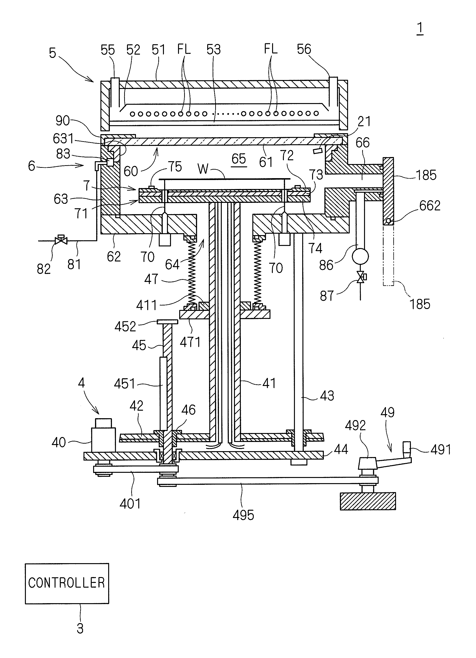
[0034]First, a general configuration of a heat treatment apparatus according to the present invention will be outlined. FIG. 1 is a longitudinal sectional view showing a configuration of a heat treatment apparatus 1 according to the present invention. The heat treatment apparatus 1 is a flash lamp annealer for irradiating a generally circular semiconductor wafer W serving as a substrate with flashes of light to heat the semiconductor wafer W.

[0035]The heat treatment apparatus 1 includes a generally cylindrical chamber 6 for receiving a semiconductor wafer W therein, and a lamp house 5 including a plurality of built-in flash lamps FL. The heat treatment apparatus 1 further includes a controller 3 for controlling operating mechanisms provided in the chamber 6 and in the lamp house 5 to cause the operating mechanisms to heat-treat a semiconductor wafer W.

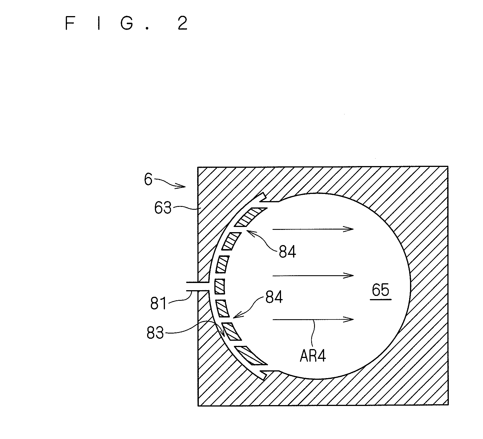
[0036]The chamber 6 is provided under the lamp house 5, and includes a chamber side portion 63 having a generally cylindrical inner w...

second preferred embodiment

[0100]Next, a second preferred embodiment according to the present invention will be described. A heat treatment apparatus in the second preferred embodiment is similar in configuration to that in the first preferred embodiment (with reference to FIGS. 1 to 7). Also, the heat treatment apparatus in the second preferred embodiment is generally similar in operation procedure to that in the first preferred embodiment (with reference to FIG. 8). For the acquisition of the table 32 according to the first preferred embodiment, the radiant energy from a semiconductor wafer W is determined from the theoretical value of black body radiation. The second preferred embodiment, however, uses a pyrometer to actually measure the radiant energy from a semiconductor wafer W.

[0101]The pyrometer is a device that senses thermal radiation from an object to be measured in a non-contacting manner to measure the temperature of the object from Equation (2). It should be noted, however, that the pyrometer, w...


PUM


Abstract

Radiant energy from a semiconductor wafer which is determined from the theoretical value of black body radiation and the actually measured result of an output from a photodiode are brought into correspondence with each other, and a table showing a correlation therebetween is acquired and stored on a magnetic disk. When a semiconductor wafer to be treated is irradiated with flashes of light from flash lamps, the photodiode receives radiant light emitted from the semiconductor wafer. A controller determines, from the output from the photodiode, the radiant energy emitted per unit time from the semiconductor wafer irradiated with flashes of light, based on the acquired table. The controller further determines the surface temperature of the semiconductor wafer from the determined radiant energy.

Description

BACKGROUND OF THE INVENTION[0001]1. Field of the Invention[0002]The present invention relates to a heat treatment apparatus and a heat treatment method for heating a thin plate-like precision electronic substrate such as a semiconductor wafer and a glass substrate for a liquid crystal display device (hereinafter referred to simply as a “substrate”) by irradiating the substrate with flashes of light.[0003]2. Description of the Background Art[0004]In the process of manufacturing a semiconductor device, impurity doping is an essential step for forming a pn junction in a semiconductor wafer. At present, it is common practice to perform impurity doping by an ion implantation process and a subsequent annealing process. The ion implantation process is a technique for causing ions of impurity elements such as boron (B), arsenic (As) and phosphorus (P) to collide against the semiconductor wafer with high acceleration voltage, thereby physically implanting the impurities into the semiconducto...

Claims


Application Information

Patent Timeline
Patent Type & Authority Applications(United States)
IPC IPC(8): F27D11/12
CPCF27B17/0025H01L21/67115H01L21/67248G01J5/0007F27B5/18G01J5/026F27D2019/0003
Inventor KUROIWA, TORU
Owner DAINIPPON SCREEN MTG CO LTD
Why Eureka
Try Eureka