Ultra high selectivity doped amorphous carbon strippable hardmask development and integration

a technology of amorphous carbon and stripping, applied in the direction of solid-state diffusion coating, semiconductor/solid-state device details, coatings, etc., can solve the problems of low selectivity of current hard-mask materials, insufficient thin resist layers to mask underlying material layers, and complex devices of integrated circuits

Active Publication Date: 2012-04-05
APPLIED MATERIALS INC
View PDF3 Cites 37 Cited by
  • Summary
  • Abstract
  • Description
  • Claims
  • Application Information

AI Technical Summary

Benefits of technology

[0012]In one another embodiment, a method of processing a substrate in a processing chamber is provided. The method includes providing a substrate in a processing chamber, flowing a hydrocarbon-containing gas mixture into the processing chamber, generating a first plasma from the hydrocarbon-containing gas mixture to deposit a boron-free amorphous carbon film on the substrate, the boron-free amorphous carbon film having a thickness between about 300 Å and about 5000 Å, stabilizing a processing condition within the processing chamber by turning off the first plasma while continuing the flow of the hydrocarbon-containing gas mixture into the processing chamber, flowing a boron-containing gas mixture into the processing

Problems solved by technology

Integrated circuits have evolved into complex devices that can include millions of transistors, capacitors and resistors on a single chip.
Such thin resist layers can be insufficient to mask underlying material layers during the

Method used


Image

  • Ultra high selectivity doped amorphous carbon strippable hardmask development and integration
  • Ultra high selectivity doped amorphous carbon strippable hardmask development and integration
  • Ultra high selectivity doped amorphous carbon strippable hardmask development and integration

Examples


Embodiment Construction

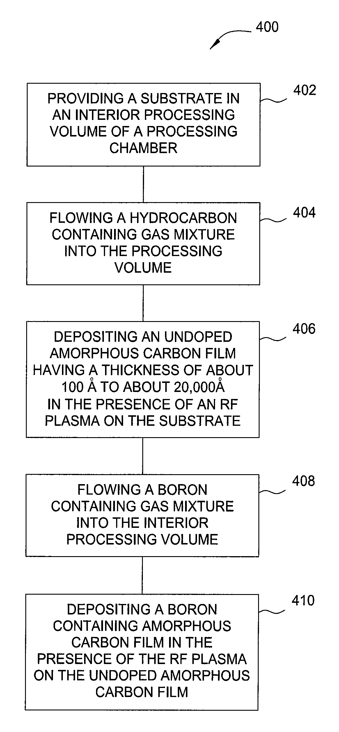
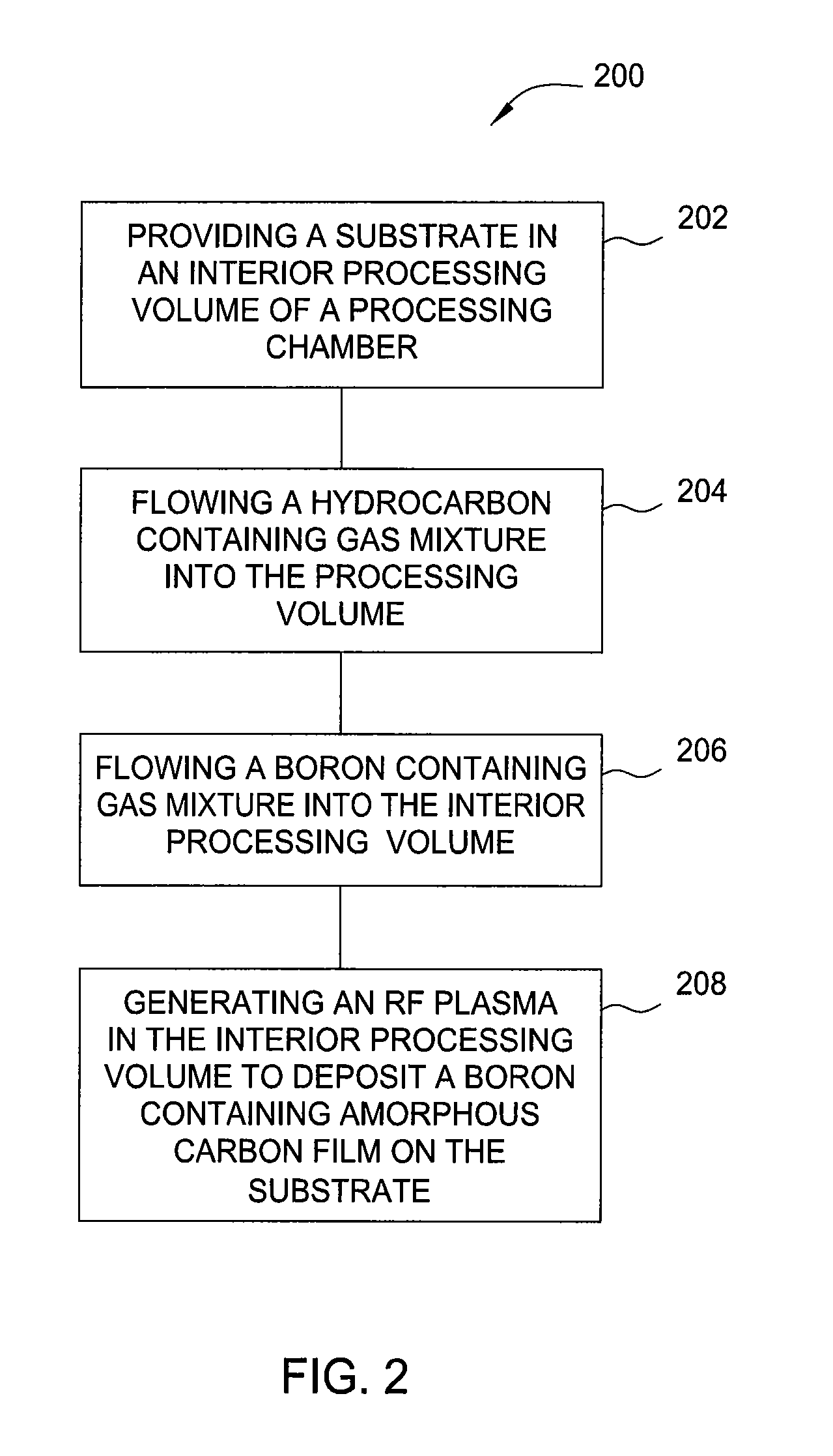
[0025]Embodiments of the present invention generally relate to the fabrication of integrated circuits and particularly to the deposition of an amorphous carbon layer on a semiconductor substrate, more particularly, to the deposition of a boron-containing amorphous carbon layer. High aspect ratio etches for deep contacts in logic and memory device structures may have aspect ratios from 10-75:1 where the hard mask is 10 to 40% of the total stack thickness. In one embodiment, a boron-containing amorphous carbon film that improves etch selectivity by 40 to 80% which would permit reducing the hardmask thickness by a similarly corresponding amount is provided. In another embodiment, a boron-containing film that is two to twenty times more etch resistant than currently know undoped amorphous carbon films allowing for a reduction in hardmask thickness and aspects of the structures is provided. Certain embodiments described herein improve the hardmask profile, critical dimension control and ...


PUM

PropertyMeasurementUnit
Fractionaaaaaaaaaa
Fractionaaaaaaaaaa
Fractionaaaaaaaaaa

Abstract

Embodiments of the present invention generally relate to the fabrication of integrated circuits and particularly to the deposition of a boron containing amorphous carbon layer on a semiconductor substrate. In one embodiment, a method of processing a substrate in a processing chamber is provided. The method comprises providing a substrate in a processing volume, flowing a hydrocarbon containing gas mixture into the processing volume, generating a plasma of the hydrocarbon containing gas mixture by applying power from an RF source, flowing a boron containing gas mixture into the processing volume, and depositing a boron containing amorphous carbon film on the substrate in the presence of the plasma, wherein the boron containing amorphous carbon film contains from about 30 to about 60 atomic percentage of boron.

Description

CROSS-REFERENCE TO RELATED APPLICATIONS[0001]This application claims benefit of U.S. provisional patent application Ser. No. 61 / 390,087, filed Oct. 5, 2010, which is herein incorporated by reference.BACKGROUND OF THE INVENTION[0002]1. Field of the Invention[0003]Embodiments of the present invention generally relate to the fabrication of integrated circuits and particularly to the deposition of a boron containing amorphous carbon layer on a semiconductor substrate.[0004]2. Description of the Related Art[0005]Integrated circuits have evolved into complex devices that can include millions of transistors, capacitors and resistors on a single chip. The evolution of chip designs continually requires faster circuitry and greater circuit density. The demands for faster circuits with greater circuit densities impose corresponding demands on the materials used to fabricate such integrated circuits. In particular, as the dimensions of integrated circuit components are reduced to the sub-micron...

Claims


Application Information

Patent Timeline
IPC IPC(8): H01L29/02C09D1/00H01L21/31
CPCC23C16/0272C23C16/26H01L21/64H01L21/02274H01L21/31144H01L21/02115H01J37/32174H01L21/02592H01L21/67276
Inventor SEAMONS, MARTIN JAYRATHI, SUDHALEE, KWANGDUK DOUGLASPADHI, DEENESHKIM, BOK HOENCHAN, CHIU
Owner APPLIED MATERIALS INC
Why Eureka
Try Eureka