Plasma processing method and plasma processing apparatus

a processing apparatus and plasma technology, applied in the field of plasma processing apparatus and plasma processing method, can solve problems such as the decrease of product yield, and achieve the effect of facilitating corrosion of chamber members and powerful oxidization ability

Active Publication Date: 2012-04-12
HITACHI HIGH-TECH CORP
View PDF5 Cites 29 Cited by
  • Summary
  • Abstract
  • Description
  • Claims
  • Application Information

AI Technical Summary

Benefits of technology

[0010]However, in an apparatus described in Japanese Patent Application Laid-Open Publication No. 11-140675, a large quantity of oxyhydride (OH) radicals is actively generated. The OH radicals have a powerful oxidization ability and facilitates corrosion of a chamber member that contains a metal. In apparatuses described in Japanese Patent Application Laid-Open Publication No. 2005-52434 and Japanese Patent Application No. 2001-176843, a reaction by-product that deposits in the processing chamber can be removed but a boron oxide remains in the processing chamber. The residue of the boron oxide and an accompanying metallic film, and slight corrosion of the chamber member have come to cause a change in a processed shape or a pattern defect along with advancement of miniaturization.
[0014]There has been a demand for cleaning during which a Ti reaction by-product can be removed using a certain general-purpose gas, and a quantity of foreign matters can be reduced without residue of a boron oxide.

Problems solved by technology

This brings about the pattern defect and invites a decrease in a product yield.

Method used


Image

  • Plasma processing method and plasma processing apparatus
  • Plasma processing method and plasma processing apparatus
  • Plasma processing method and plasma processing apparatus

Examples


first embodiment

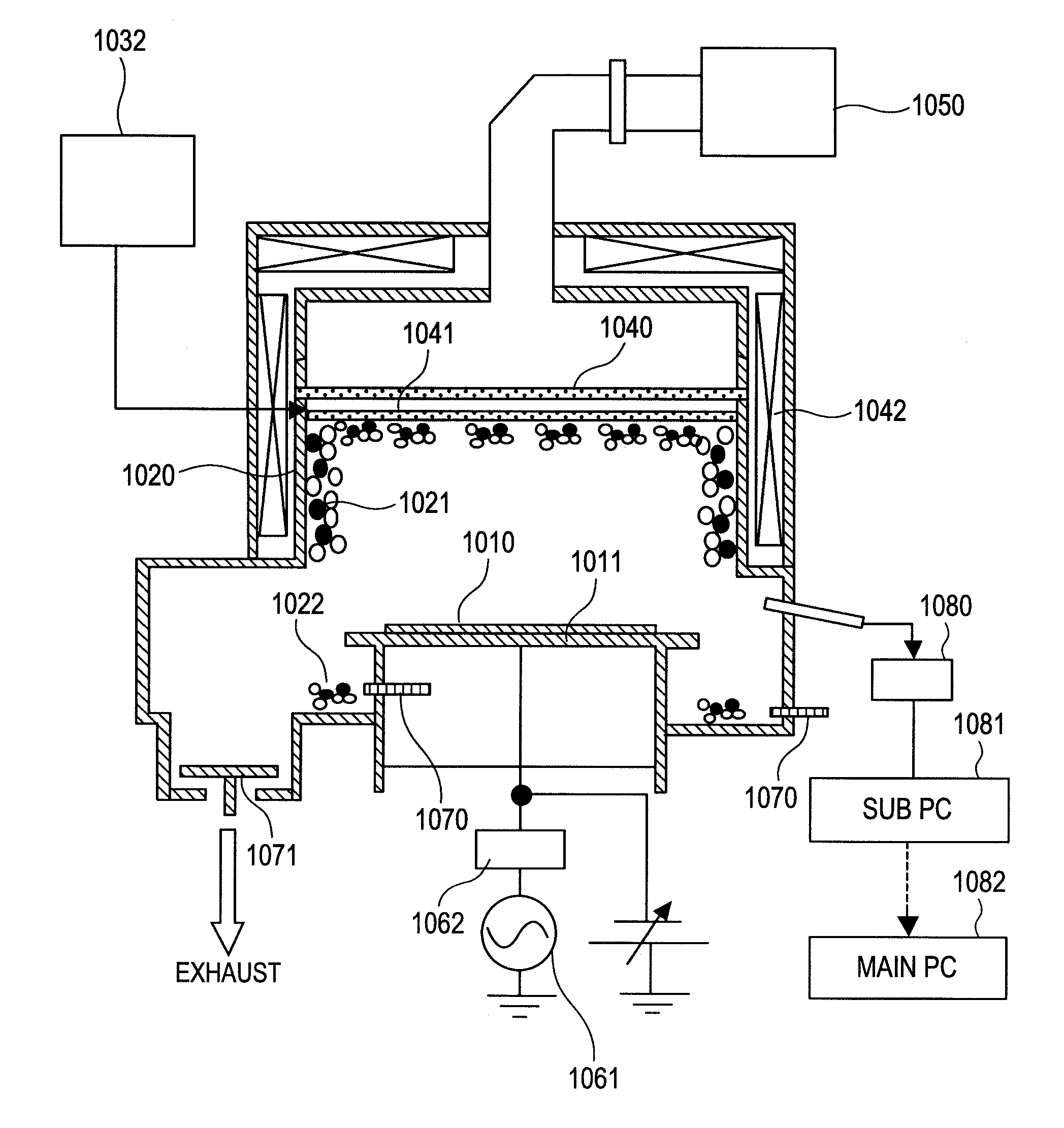
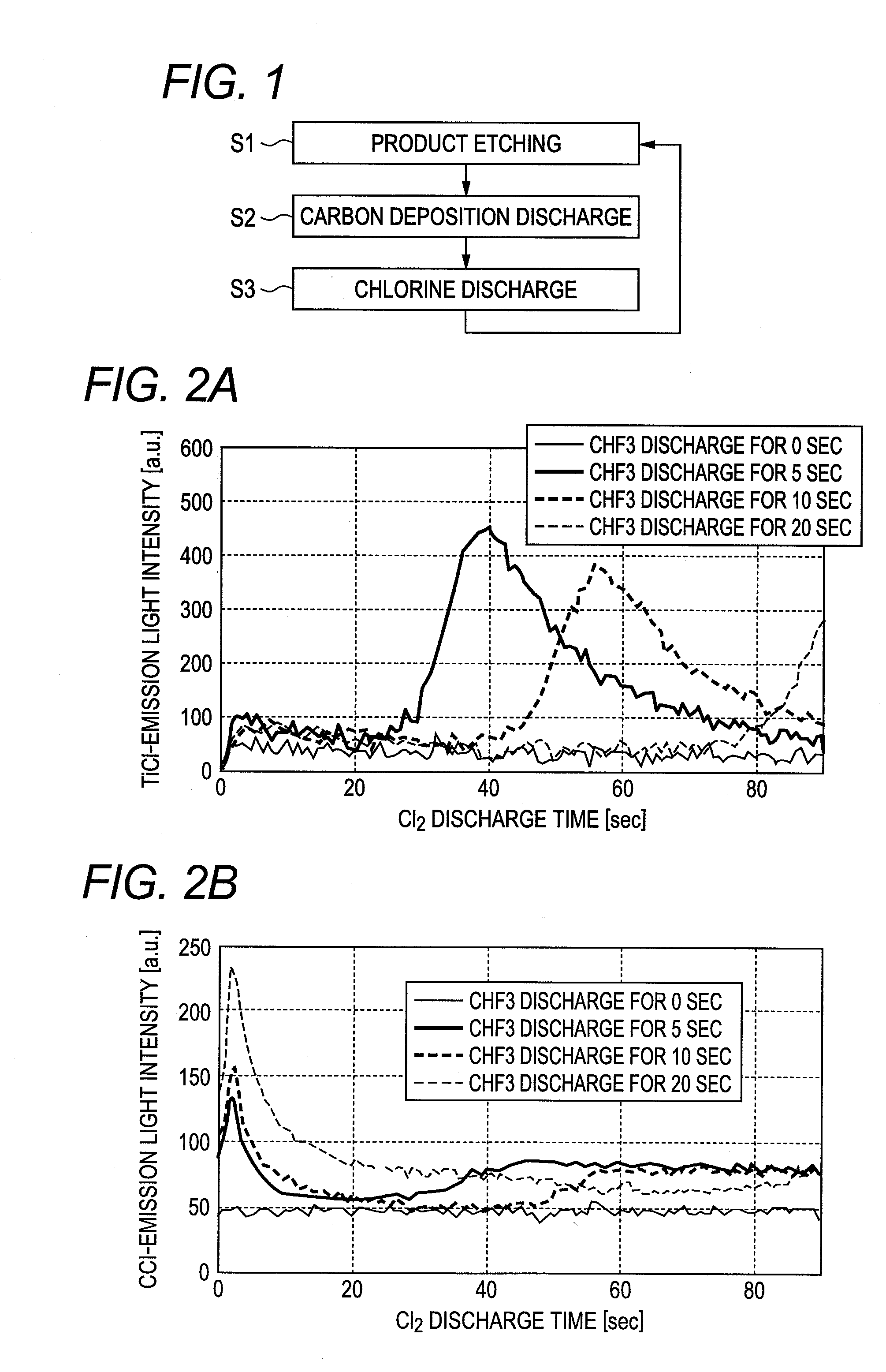
[0031]A first embodiment of the present invention will be described in conjunction with FIG. 1 to FIG. 5 and FIG. 10. FIG. 10 is a schematic constitution diagram of a plasma processing apparatus employed in the present embodiment.

[0032]To begin with, the plasma processing apparatus employed in the present embodiment will be described below. The plasma processing apparatus (etching apparatus) shown in FIG. 10 includes an electrode 1011 on which a wafer 1010 is placed and which is disposed in a processing container, a gas feeder 1032, a top panel 1040, a shower plate 1041, an electromagnet 1042, a high-frequency waveguide 1050, a radiofrequency bias power supply 1061, a matching box 1062, a vacuum exhaust valve 1071 of a processing chamber, an emission spectroscope 1080, a unit in which an emission spectrum or data obtained by the emission spectroscope 1080 is stored (for example, a sub-personal computer (PC) 1081), and a main PC 1082 that controls the etching apparatus. The main PC 1...

second embodiment

[0044]A second embodiment of the present invention will be described in conjunction with FIG. 6, FIG. 7, and FIG. 9. Incidentally, information that has been described in relation to the first embodiment but will not be described in relation to the present embodiment can be applied to the present embodiment unless exceptional circumstances arise.

[0045]In relation to the first embodiment, a description has been made of that Ti deposited on the surface of the processing chamber can be cleaned out by performing the process S3 of chlorine-series discharge immediately after completion of the process S2 of carbon-series deposition discharge. However, if a Ti reaction by-product is thickly deposited on the surface of the processing chamber during product etching (process S1), or if the Ti reaction by-product is thickly deposited because the product etching has already been repeated plural times, the deposit of the Ti reaction by-product cannot be fully cleaned out by once performing the pro...

third embodiment

[0053]A third embodiment of the present invention will be described below in conjunction with FIG. 8. Incidentally, information that has been described in relation to the first or second embodiment but will not be described in relation to the present embodiment can be applied to the present embodiment unless exceptional circumstances arise.

[0054]FIG. 8 is a flowchart describing a procedure employed in a plasma processing method in accordance with the present embodiment. In the present embodiment, a process S2′ of oxygen discharge is inserted between product etching (process S1) and carbon-series deposition discharge (process S2) which are described in relation to the first embodiment by referring to FIG. 1). An effect of the oxygen discharge will be described below.

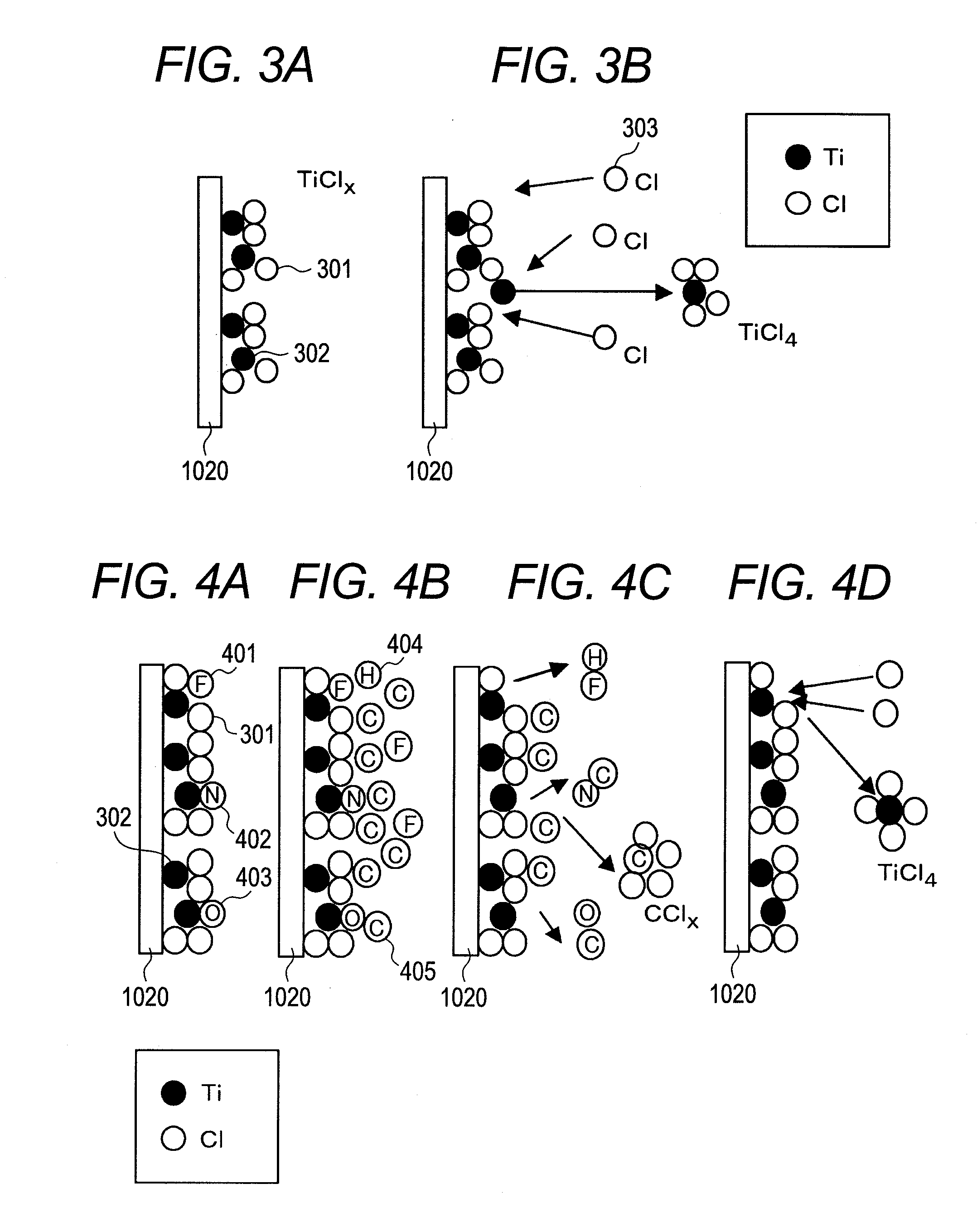
[0055]As seen from Table 1, comparison of binding energies between Ti and N, between Ti and Cl, between Ti and F, and between Ti and O with one another demonstrates that the binding energy between Ti and O is highest. In ...


PUM

PropertyMeasurementUnit
melting pointaaaaaaaaaa

Abstract

Provided is a plasma processing method capable of removing a Ti-series deposit from the surface of a processing chamber of a plasma processing apparatus without production of a foreign matter such as a boron oxide. The plasma processing method includes carbon-series deposition discharge which succeeds product etching during which a sample containing a Ti material is processed, and during which a carbon-series film is deposited on a Ti reaction by-product deposited on the surface of the processing chamber, and chlorine-series discharge which succeeds the carbon-series deposition discharge and during which the carbon-series film and Ti that are deposited on the surface of the processing chamber are removed.

Description

CLAIM OF PRIORITY[0001]The present application claims priority from Japanese patent application JP 2010-227640 filed on Oct. 7, 2010, the content of which is hereby incorporated by reference into this application.BACKGROUND OF THE INVENTION[0002]1. Field of the Invention[0003]The present invention relates to a plasma processing apparatus and a plasma processing method which are employed in fabrication of semiconductor devices.[0004]2. Description of the Related Art[0005]Along with a recent tendency of semiconductor integrated circuits to high-density integration and high-processing speed performance, a gate electrode is requested to be further miniaturized. According to the International Technology Roadmap for Semiconductors 2008 Edition, a dimension of a gate of a 40 nm-node high-speed logic device has reached 22 nm in 2011, and precision in a processed dimension is requested to be equal to or smaller than 1.33 nm (3σ). In generations succeeding the 45 nm node, an existing silicon ...

Claims


Application Information

Patent Timeline
Patent Type & Authority Applications(United States)
IPC IPC(8): B08B7/00H05H1/24B08B13/00
CPCH01J37/32192H01L21/205H01L21/3065
Inventor HIROTA, KOUSA
Owner HITACHI HIGH-TECH CORP
Why Eureka
Try Eureka