Nitride-based semiconductor laser element and optical apparatus

a laser element and semiconductor technology, applied in semiconductor lasers, lasers, laser details, etc., can solve the disadvantageous instability of the laser beam intensity, and achieve the effects of reducing the stress on the first and second dielectric films close to the emitting cavity facet, preventing separation, and facilitating inhibition

Inactive Publication Date: 2012-04-19
SANYO ELECTRIC CO LTD
View PDF3 Cites 9 Cited by
  • Summary
  • Abstract
  • Description
  • Claims
  • Application Information

AI Technical Summary

Benefits of technology

[0026]In this case, the thickness of at least either the first dielectric film or the second dielectric film is preferably smaller than the thickness of at least either the sixth dielectric film or the seventh dielectric film. According to this structure, stress on at least either the first dielectric film or the second dielectric film close to the emitting-side cavity facet can be relatively reduced as compared with stress on at least either the sixth dielectric film or the seventh dielectric film. Thus, the first and second dielectric films, easily altered due to concentration of heat energy or light energy, can be inhibited from separation even if the facet coating film further includes the sixth and seventh dielectric films.
[0027]In the aforementioned structure having the facet coating film further including the sixth and seventh dielectric films, the thickness of each of the first dielectric film and the second dielectric film is preferably smaller than the thickness of each of the third dielectric film, the fourth dielectric film, the fifth dielectric film, the sixth dielectric film and the seventh dielectric film. According to this structure, stress on the first and second dielectric films close to the emitting-side cavity facet can be relatively reduced. Thus, the first and second dielectric films, easily altered due to concentration of heat energy or light energy, can be easily inhibited from separating from the emitting-side cavity facet.
[0028]In the aforementioned structure having the facet coating film further including the sixth and seventh dielectric films, the thickness of the seventh dielectric film is preferably larger than the thickness of the sixth dielectric film. According to this structure, stress, relatively larger than that on the seventh dielectric film, on the sixth dielectric film made of aluminum nitride can be so reduced that the adhesiveness between the sixth and seventh dielectric films can be improved. Thus, the sixth and seventh dielectric films can be inhibited from separating from each other in the facet coating film.
[0029]In the aforementioned structure having the facet coating film further including the sixth and seventh dielectric films, the sixth dielectric film made of the aluminum oxynitride is preferably expressed as AlOxNy (where 0≦x<1.5 and 0<y<1), and preferably satisfies the relation x<y in the AlOxNy. According to this structure, the quantity of oxygen contained in the sixth dielectric film and diffused into the fifth dielectric film can be easily reduced.
[0030]In the aforementioned structure having the facet coating film further including the sixth and seventh dielectric films, the second dielectric film is preferably in contact with a surface of the first dielectric film opposite to the emitting-side cavity facet, the third dielectric film is preferably in contact with a surface of the second dielectric film opposite to the first dielectric film, the fourth dielectric film is preferably in contact with a surface of the third dielectric film opposite to the second dielectric film, the fifth dielectric film is preferably in contact with a surface of the fourth dielectric film opposite to the third dielectric film, the sixth dielectric film is preferably in contact with a surface of the fifth dielectric film opposite to the fourth dielectric film, and the seventh dielectric film is preferably in contact with a surface of the sixth dielectric film opposite to the fifth dielectric film. According to this structure, the adhesiveness between the dielectric films is so improved that the facet coating film can be reliably inhibited from separating from the emitting-side cavity facet.
[0031]In the aforementioned nitride-based semiconductor laser element according to the first aspect, the semiconductor element layer preferably has a principal surface consisting of an approximately (0001) plane of the nitride-based semiconductor, the light-emitting layer preferably includes an active layer, the nitride-based semiconductor laser element preferably further includes a ridge portion for forming a waveguide on the active layer of the semiconductor element layer, and the ridge portion preferably extends along an approximately [1-100] direction of the semiconductor element layer. According to this structure, the facet coating film according to the present invention can be easily formed on the emitting-side cavity facet consisting of an approximately (1-100) plane.

Problems solved by technology

Consequently, the reflectance on the cavity facet so fluctuates that the intensity of a laser beam is disadvantageously unstabilized.

Method used


Image

  • Nitride-based semiconductor laser element and optical apparatus
  • Nitride-based semiconductor laser element and optical apparatus
  • Nitride-based semiconductor laser element and optical apparatus

Examples


first embodiment

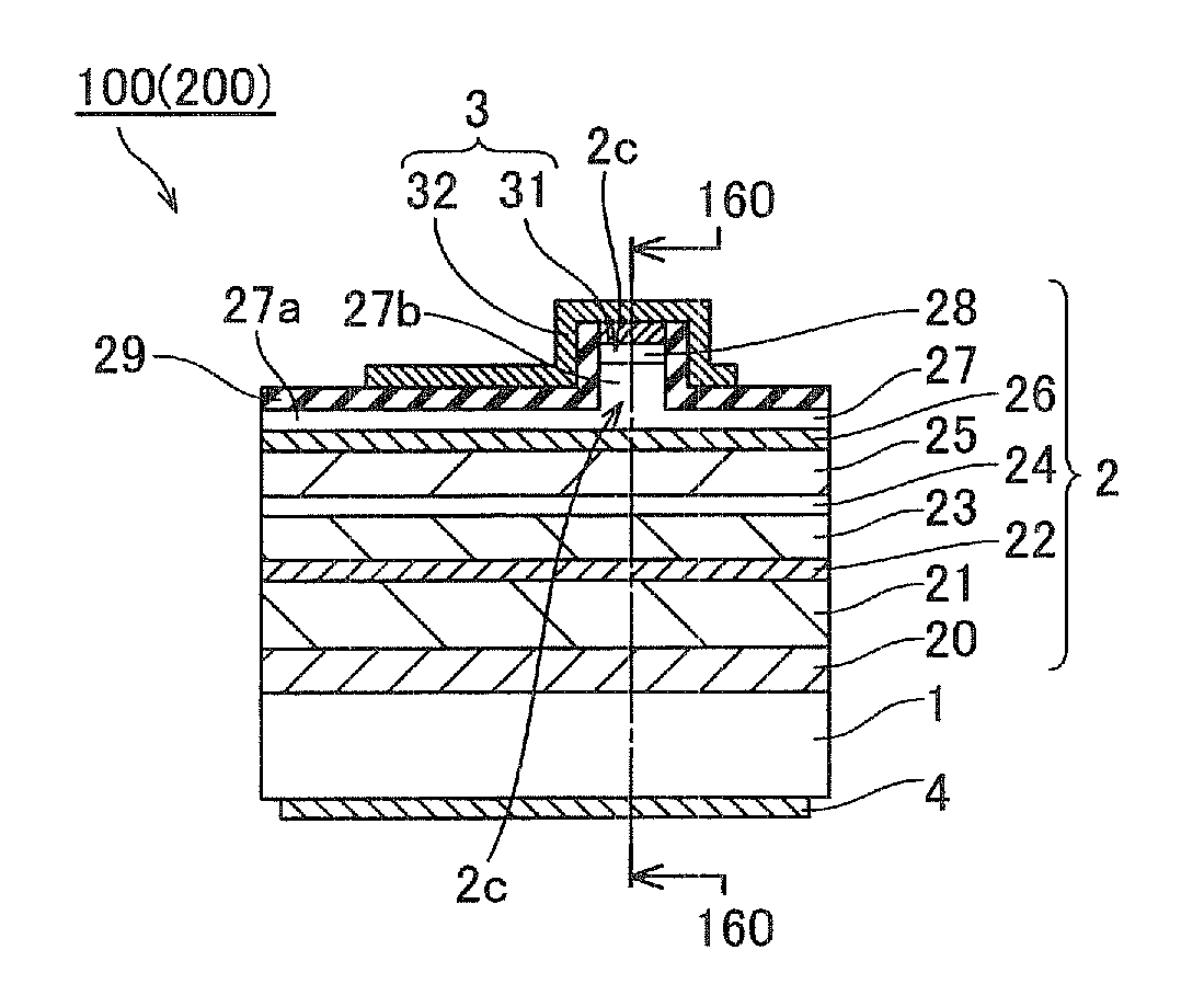
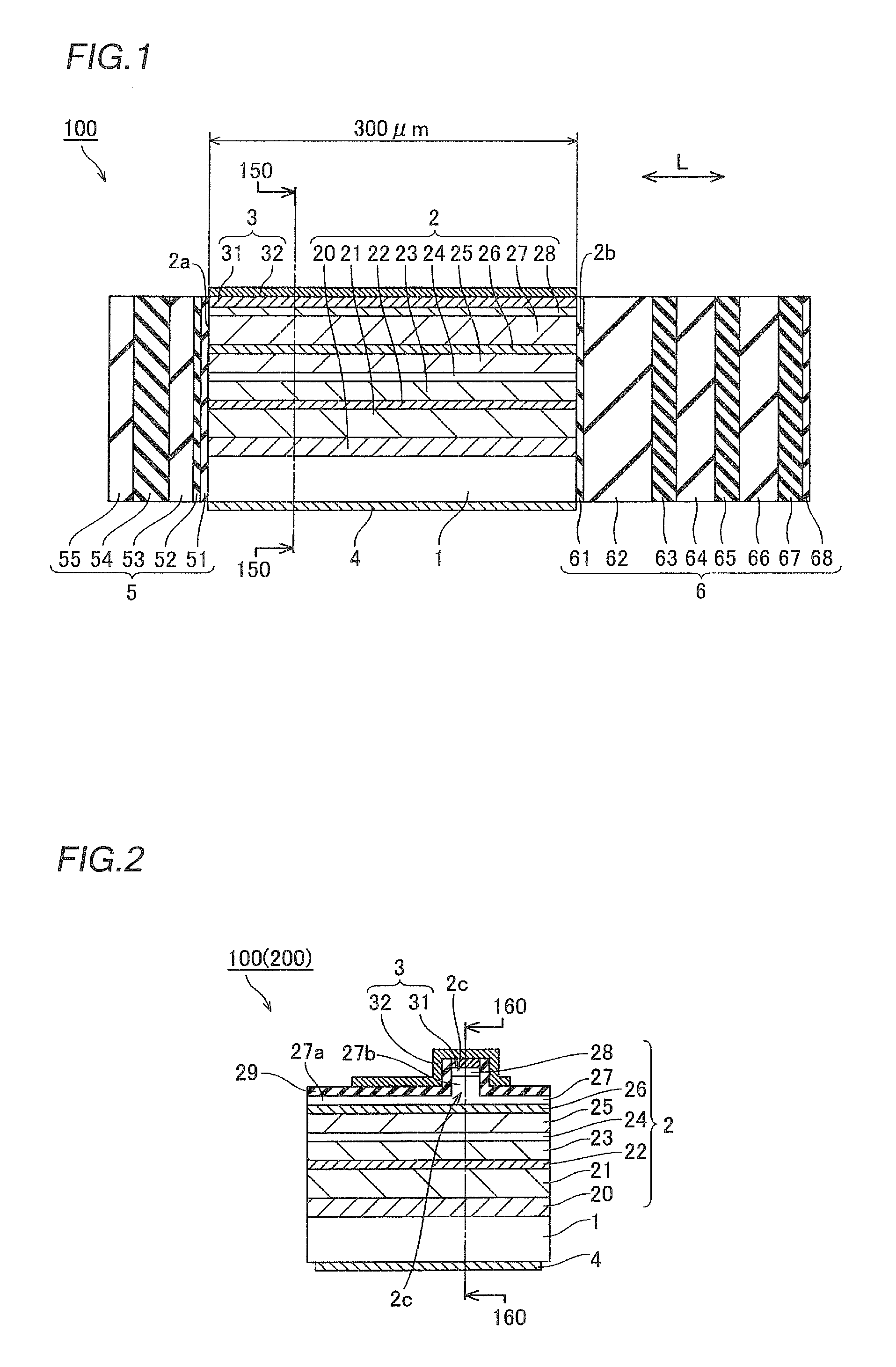
[0040]A nitride-based semiconductor laser element 100 according to a first embodiment of the present invention has a lasing wavelength of about 405 nm, and includes a semiconductor element layer 2 made of a nitride-based semiconductor formed on the upper surface (approximately (0001) Ga plane) of a substrate 1 made of n-type GaN, a p-side electrode 3 formed on the semiconductor element layer 2 and an n-side electrode 4 formed on the lower surface (approximately (0001) N plane) of the substrate 1, as shown in FIGS. 1 and 2. The semiconductor element layer 2 is provided with a pair of cavity facets, i.e., an emitting-side cavity facet 2a and a reflecting-side cavity facet 2b, orthogonal to a light-emitting direction (direction L (approximately [1-100] direction)). In other words, the pair of cavity facets 2a and 2b consist of approximately (1-100) planes. FIG. 1 shows a section, taken along the line 160-160 in FIG. 2, of the nitride-based semiconductor laser element 100 in a direction...

second embodiment

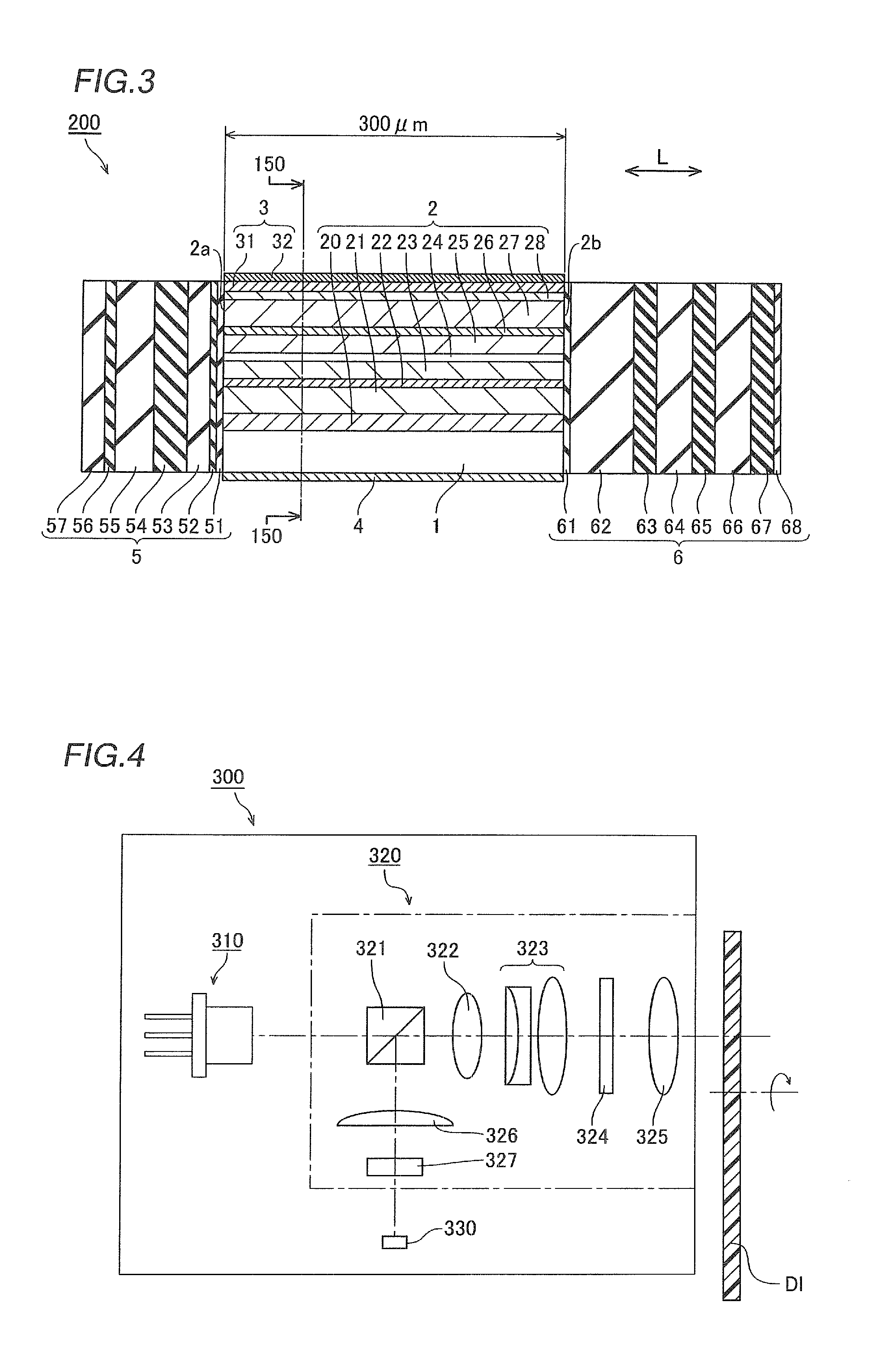
[0071]The structure of a nitride-based semiconductor laser element 200 according to a second embodiment of the present invention is described with reference to FIG. 3. FIG. 3 shows a section of the nitride-based semiconductor laser element 200 parallel to a laser beam emitting direction (direction L).

[0072]In the nitride-based semiconductor laser element 200, the structure of a first facet coating film 5 on an emitting-side cavity facet 2a is different from that of the first facet coating film 5 of the nitride-based semiconductor laser element 100 in a point that an Al2O3 layer 53, an AlOxNy layer 54 and an Al2O3 layer 55 have thicknesses of about 33 nm, about 56 nm and about 65 nm respectively. An AlOxNy layer 56 (0≦x2O3 layer 55 opposite to the AlOxNy layer 54, while an Al2O3 layer 57 having a thickness of about 38 nm is formed in contact with a surface of the AlOxNy layer 56 opposite to the Al2O3 layer55. Referring to the AlOxNy layer 56, x and y represent atomic ratios of oxygen...

third embodiment

[0077]The structure of an optical pickup apparatus 300 according to a third embodiment of the present invention is now described with reference to FIG. 4. The optical pickup apparatus 300 is an example of the “optical apparatus” in the present invention.

[0078]The optical pickup apparatus 300 includes a three-wavelength semiconductor laser device 310, an optical system 320 adjusting laser beams emitted from the three-wavelength semiconductor laser device 310 and a light detection portion 330 receiving the laser beams, as shown in FIG. 4.

[0079]The three-wavelength semiconductor laser device 310 is loaded with the aforementioned nitride-based semiconductor laser element 200 and a red / infrared two-wavelength semiconductor laser element (not shown) emitting a red laser beam having a wavelength of about 650 nm and an infrared laser beam having a wavelength of about 780 nm, and can separately emit laser beams of three wavelengths.

[0080]The optical system 320 has a polarized beam splitter (...


PUM


Abstract

This nitride-based semiconductor laser element includes a semiconductor element layer made of a nitride-based semiconductor having an emitting-side cavity facet and a reflecting-side cavity facet, and a facet coating film formed on the emitting-side cavity facet. The facet coating film has a first dielectric film made of aluminum nitride formed in contact with the emitting-side cavity facet, a second dielectric film made of aluminum oxynitride formed on a side of the first dielectric film opposite to the emitting-side cavity facet, a third dielectric film made of aluminum oxide formed on a side of the second dielectric film opposite to the first dielectric film, a fourth dielectric film made of aluminum oxynitride formed on a side of the third dielectric film opposite to the second dielectric film, and a fifth dielectric film made of aluminum oxide formed on a side of the fourth dielectric film opposite to the third dielectric film.

Description

CROSS-REFERENCE TO RELATED APPLICATION[0001]The priority application number JP2010-231045, Nitride-Based Semiconductor Laser Element and Optical Apparatus, Oct. 14, 2010, Yoshiki Murayama, upon which this patent application is based is hereby incorporated by reference.BACKGROUND OF THE INVENTION[0002]1. Field of the Invention[0003]The present invention relates to a nitride-based semiconductor laser element and an optical apparatus, and more particularly, it relates to a nitride-based semiconductor laser element and an optical apparatus each having dielectric films formed on an emitting-side cavity facet.[0004]2. Description of the Background Art[0005]In recent years, a semiconductor laser has been widely employed as a light source for an optical disk system or an optical communication system. Following improvement in performance of apparatuses constituting the system, improvement in laser element characteristics is desired. In particular, wavelength shortening of a laser beam and a ...

Claims


Application Information

Patent Timeline
Patent Type & Authority Applications(United States)
IPC IPC(8): H01S5/02
CPCB82Y20/00H01S5/4087H01S5/34333H01S5/0287
Inventor MURAYAMA, YOSHIKI
Owner SANYO ELECTRIC CO LTD
Why Eureka
Try Eureka