Deposition-free sealing for Micro- and Nano-fabrication

a technology of micro- and nano-fabrication, applied in the field of micro- and nano-scale packaging of semiconductor devices, can solve the problem of low surface potential

Inactive Publication Date: 2012-05-03
THE BOARD OF TRUSTEES OF THE LELAND STANFORD JUNIOR UNIV
View PDF3 Cites 9 Cited by
  • Summary
  • Abstract
  • Description
  • Claims
  • Application Information

AI Technical Summary

Benefits of technology

[0021]The present invention enables microsystem die that are encapsulated in a single step at t

Problems solved by technology

Silicon migration, however, seeks to attain uniform

Method used


Image

  • Deposition-free sealing for Micro- and Nano-fabrication
  • Deposition-free sealing for Micro- and Nano-fabrication
  • Deposition-free sealing for Micro- and Nano-fabrication

Examples


Embodiment Construction

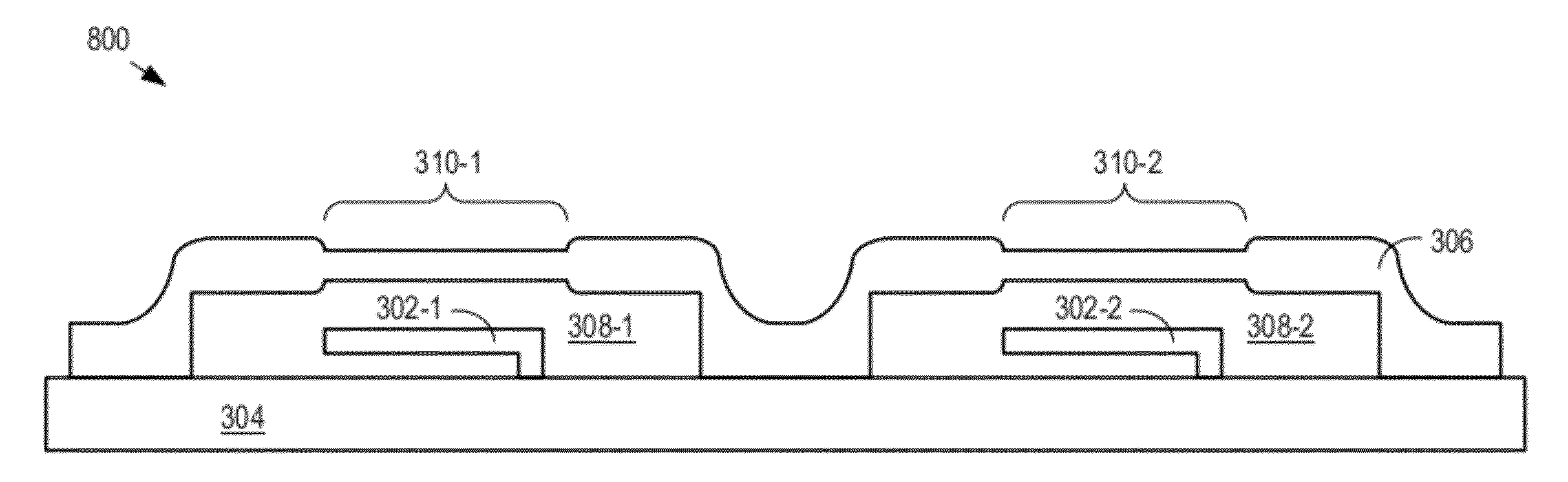
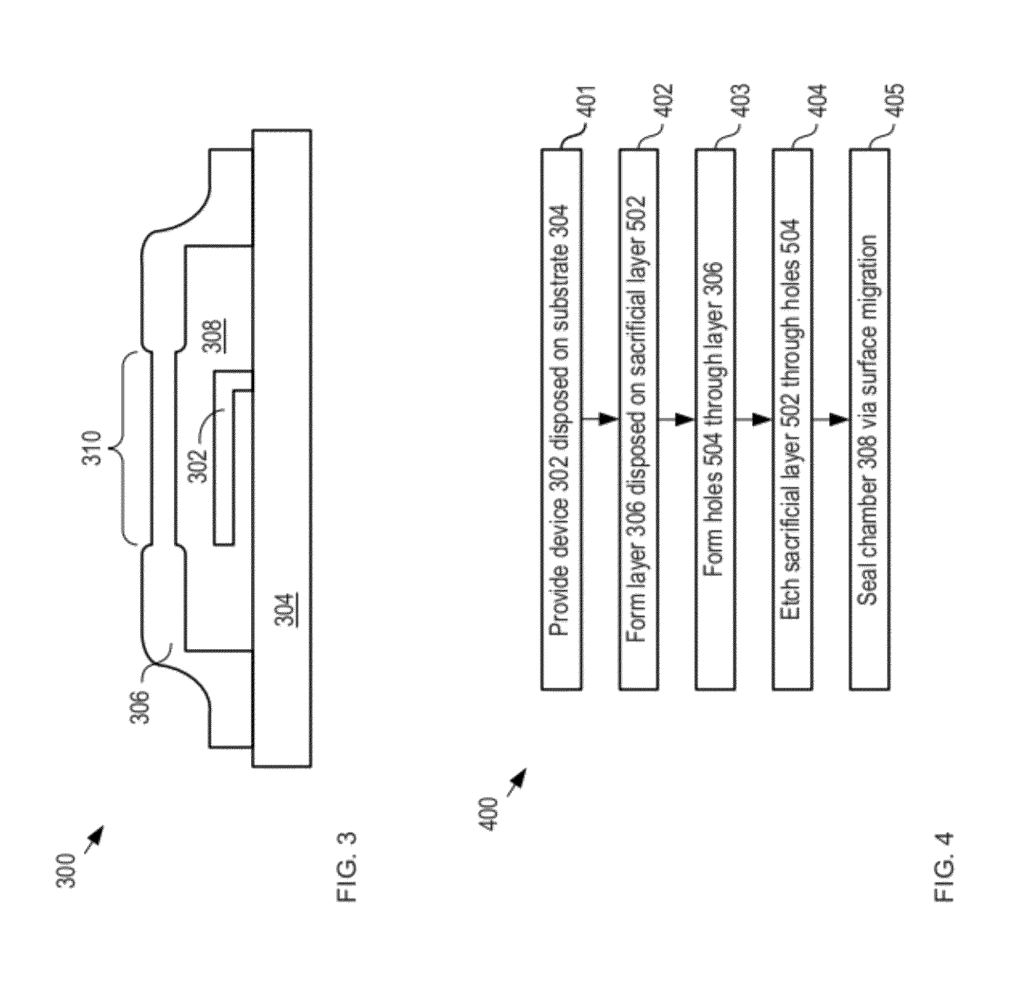
[0041]Single-step, wafer-scale vacuum packaging can greatly simplify packaging processes for MEMS / NEMS, improve device reliability, and reduce production costs. The present invention exploits the phenomenon of surface migration, wherein surface atoms migrate along an exposed surface in an attempt to minimize surface energy. Sharp features, such as corners, are characterized by relatively high surface energy. Surface migration, therefore, can be employed to reduce the sharpness of such features and even attain substantially uniform surface curvature. As a result, it can lead to significant three-dimensional shape transformations, such as the splitting or joining of surfaces, rounding of feature corners, or reshaping of columnar pillars into rounded projections.

[0042]Silicon migration offers an alternative for sealing release through-holes that mitigates or eliminates some of the problems associated with prior-art encapsulation techniques described above. For the purposes of this Spec...


PUM


Abstract

A method for sealing through-holes in a material via material diffusion, without the deposition of a sealant material, is disclosed. The method is well suited to the fabrication and packaging of microsystems technology-based devices and systems. In some embodiments, the method comprises forming sacrificial material release through-holes through a structural layer, removing the sacrificial material via an etch that etches the sacrificial material through the release through-holes, and sealing of the release through-holes via material diffusion.

Description

CROSS REFERENCE TO RELATED APPLICATIONS[0001]This application claims priority of provisional patent application U.S. Ser. No. 61 / 408,007, filed Oct. 29, 2010 (Attorney Docket 146-021US), the entire contents of which are herein incorporated by reference.STATEMENT REGARDING FEDERALLY-SPONSORED RESEARCH[0002]This invention was made with Government support under contract HR0011-06-1-0049 awarded by the Defense Advanced Research Projects Agency. The Government has certain rights in the invention.FIELD OF THE INVENTION[0003]The present invention relates to semiconductor fabrication in general, and, more particularly, to semiconductor, micro-scale, and nano-scale packaging.BACKGROUND OF THE INVENTION[0004]Advances in Micro Electro Mechanical Systems (MEMS) technology have led to the development of devices and systems that have become ubiquitous in many markets, such as automotive, medical, consumer products, military hardware, and telecommunications. More recently, nanotechnology has begun...

Claims


Application Information

Patent Timeline
IPC IPC(8): H01L23/20H01L21/768
CPCB81C2201/0116B81C1/00333
Inventor KANT, RISHIHOWE, ROGER THOMAS
Owner THE BOARD OF TRUSTEES OF THE LELAND STANFORD JUNIOR UNIV
Why Eureka
Try Eureka