High melting point soldering layer and fabrication method for the same, and semiconductor device

a high melting point and soldering layer technology, applied in the direction of manufacturing tools, solvents, transportation and packaging, etc., can solve the problems of spoiled sic devices, inability to drive at high temperature, and inability to use sic devices, etc., to achieve high melting point, high melting point, and high melting point soldering layers

Active Publication Date: 2012-05-10
ROHM CO LTD +1
View PDF2 Cites 58 Cited by
  • Summary
  • Abstract
  • Description
  • Claims
  • Application Information

AI Technical Summary

Benefits of technology

[0024]According to the present invention, it can be provided with the binary based high melting point soldering layer having the TLP bonding of the high melting point according to the low temperature processing, and the fabrication method for the same.
[0025]Moreover, according to the present invention, it can be provided with the semiconductor device to which the high melting point soldering layer is applied.

Problems solved by technology

However, since the SIC devices can theoretically operate to about 400 degrees C., if the SIC devices are driven at high temperature when using the conventional low melting point solder, the short circuit between electrodes, the delamination between the SiC devices and a base plate, etc. occurred by fusing bonding parts when using the low melting point solder, and then the reliability of the SiC devices are spoiled.
Accordingly, the SiC devices could not be driven at high temperature, and the characteristic of the SiC devices was not able to be used.
Since the TLP bonding of three kinds or four kinds of metallic materials is used as a result, the components of the mixed crystal of the conductive metal are complicated.

Method used


Image

  • High melting point soldering layer and fabrication method for the same, and semiconductor device
  • High melting point soldering layer and fabrication method for the same, and semiconductor device
  • High melting point soldering layer and fabrication method for the same, and semiconductor device

Examples


first embodiment

(Configuration of High Melting Point Soldering Layer)

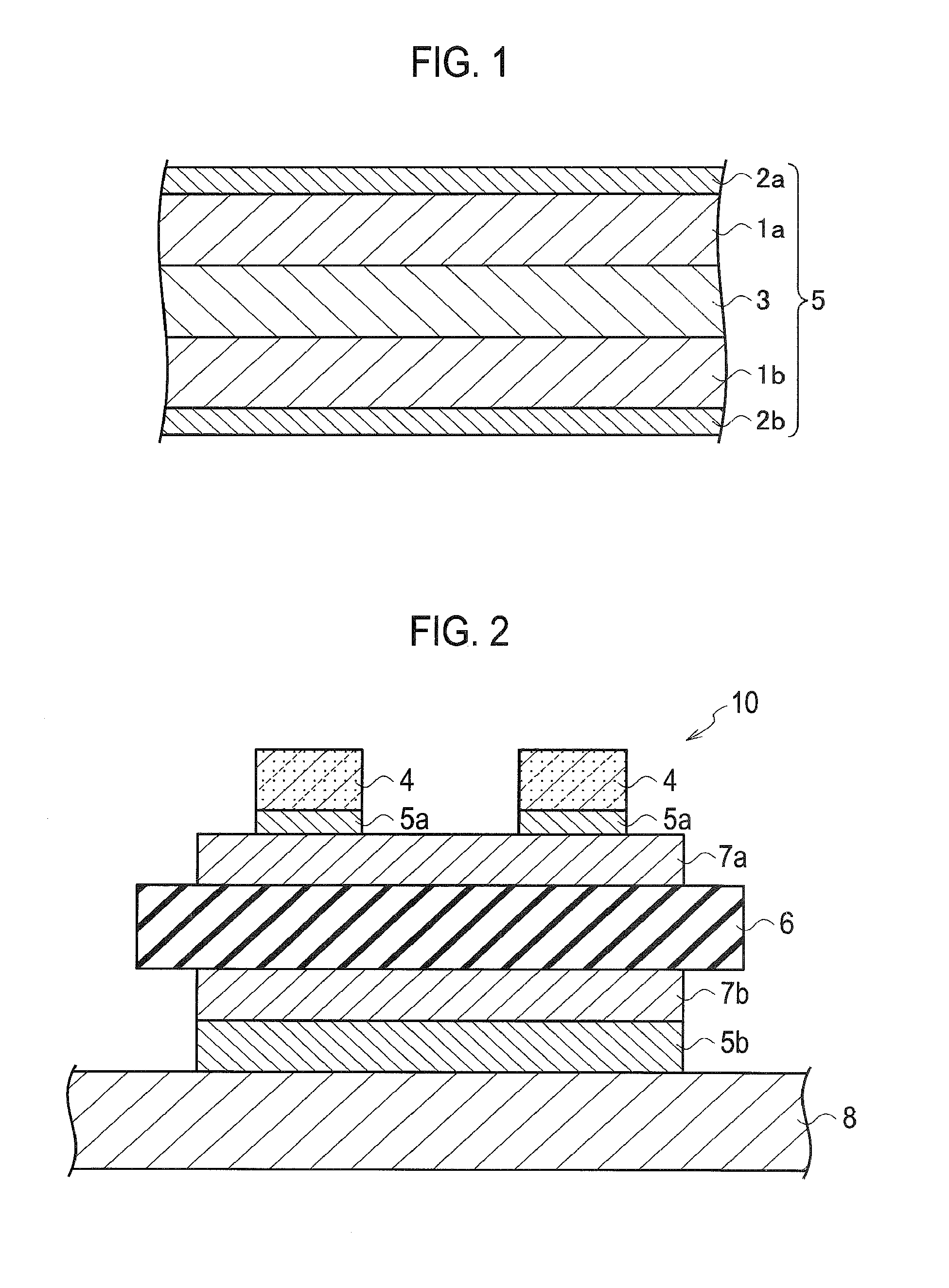
[0049]As shown in FIG. 1, a high melting point soldering layer 5 according to a first embodiment includes: a low melting point metal layer 3; a first high melting point metal layer 1a disposed on the surface of the low melting point metal layer 3; and a second high melting point metal layer 1b disposed at the back side of the low melting point metal layer 3. The low melting point metal layer 3, the first high melting point metal layer 1a, and the second high melting point metal layer 1b are mutually alloyed by TLP bonding.

[0050]As a result, as for a melting point of the high melting point soldering layer 5 according to the first embodiment, a melting point between a melting points of the low melting point metal layer 3 and a melting point of the first high melting point metal layer 1a and / or the second high melting point metal layer 1b is obtained.

[0051]The low melting point metal layer 3 is formed with a Sn layer or a Sn—Ag eutec...

modified example

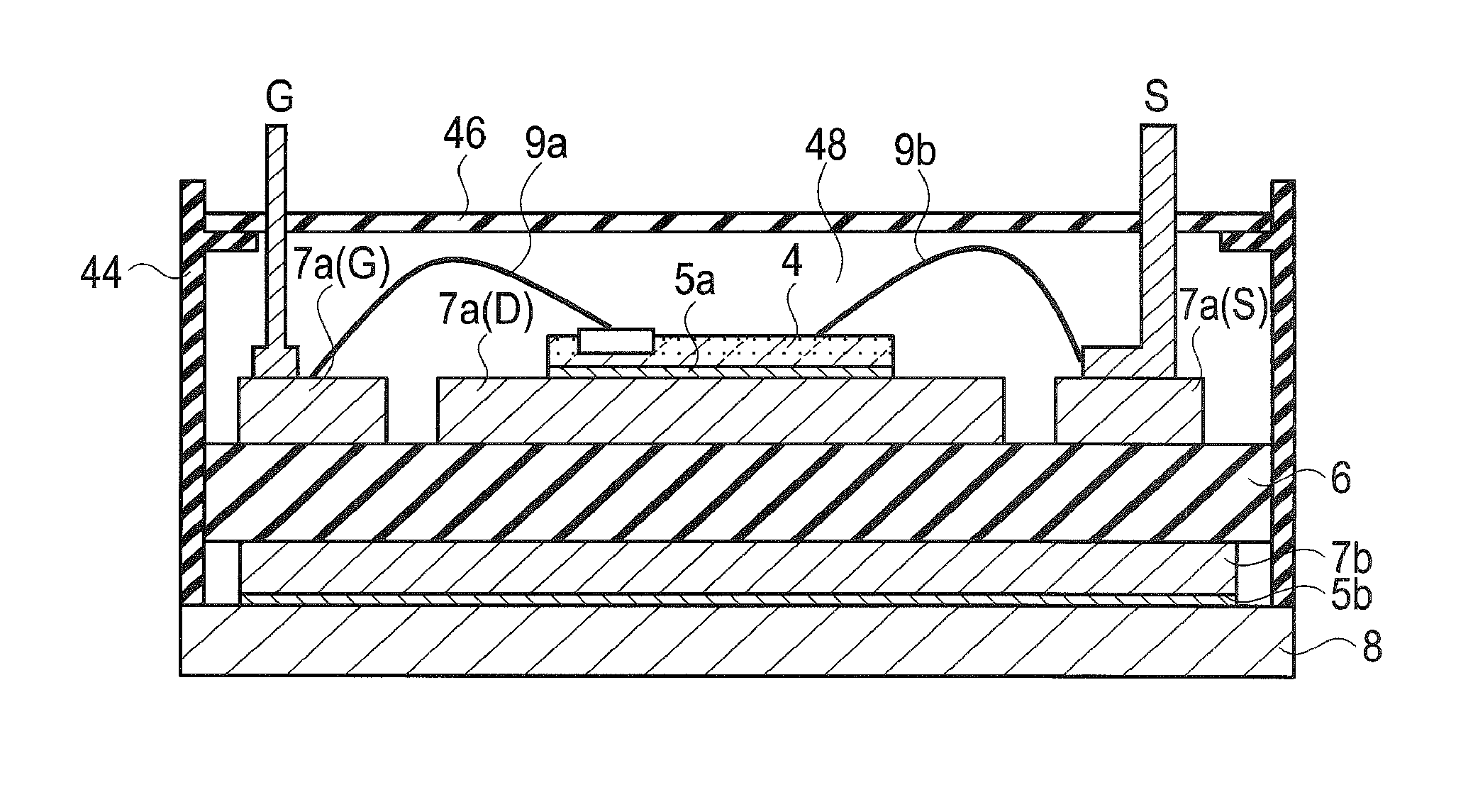
[0120]A schematic bird's-eye view configuration of a semiconductor device 10 according to a modified example of the first embodiment is expressed as shown in FIG. 18A, and a schematic cross-section structure taken in the line I-I of FIG. 18A is expressed as shown in FIG. 18B. In the semiconductor device 10 according to the modified example of the first embodiment shown in FIG. 18, three semiconductor devices are connected in parallel.

[0121]As shown in FIG. 18A and FIG. 18B, the semiconductor device 10 according to the modified example of the first embodiment includes: a semiconductor device 4; a third high melting point soldering layer 5c disposed on the semiconductor device 4; a source side pad electrode 40 disposed on the third high melting point soldering layer 5c; a fourth high melting point soldering layer 5d disposed at the back side of the semiconductor device 4 of the opposite side of the surface where the third high melting point soldering layer 5c is disposed; and a drain ...


PUM

PropertyMeasurementUnit
thicknessaaaaaaaaaa
thicknessaaaaaaaaaa
mechanical pressureaaaaaaaaaa

Abstract

A high melting point soldering layer includes a low melting point metal layer, a first high melting point metal layer disposed on a surface of the low melting point metal layer, and a second high melting point metal layer disposed at a back side of the low melting point metal layer. The low melting point metal layer, the first high melting point metal layer, and the second high melting point metal layer are mutually alloyed by transient liquid phase bonding, by annealing not less than a melting temperature of the low melting point metal layer, diffusing the metal of the low melting point metal layer into an alloy of the first high melting point metal layer and the second high melting point metal layer. The high melting point soldering layer has a higher melting point temperature than that of the low melting point metal layer. It is provided a binary based high melting point soldering layer having TLP bonding of a high melting point according to a low temperature processing, a fabrication method for the high melting point soldering layer and a semiconductor device to which the high melting point soldering layer is applied.

Description

TECHNICAL FIELD[0001]The present invention relates to a high melting point soldering layer, a fabrication method for the high melting point soldering layer, and a semiconductor device. More specifically, the present invention relates to a high melting point soldering layer fabricated by TLP (Transient Liquid Phase) bonding, a fabrication method for the high melting point soldering layer, and a semiconductor device.BACKGROUND[0002]Currently, research and development of an SiC (Silicon Carbide) device are done in many research institutions. As a characteristic of the SiC devices, it can be mentioned of low on resistance, high speed switching, high temperature operation, etc.[0003]Conventionally, since the temperature span which can operate in Si devices, such as IGBTs (Insulated Gate Bipolar Transistors), currently used in the field of a semiconductor power module is to about 150 degrees C., it was possible to have driven even when using low melting point solder, such as a conventiona...

Claims


Application Information

Patent Timeline
Patent Type & Authority Applications(United States)
IPC IPC(8): H01L23/498B32B15/01B23K1/20H01L29/02H01L23/492
CPCY10T428/12708H01L2924/1461H01L2924/3841H01L2924/01327H01L2924/13055H01L2224/32238H01L2224/32227H01L2924/1305B23K1/0016B23K35/0238B23K35/262B23K35/3006B23K2201/40B32B15/018H01L23/3735H01L23/488H01L2224/85H01L2924/13091H01L2224/48091H01L2224/48105H01L2224/48229H01L2224/73265H01L2224/83101H01L2224/83204H01L2224/83211H01L2224/83801H01L2224/83825H01L2224/92147H01L2924/01322H01L2224/29155H01L2224/271H01L23/053H01L24/29H01L24/32H01L24/48H01L24/83H01L24/85H01L25/0655H01L2224/2908H01L2224/29111H01L2224/29139H01L2924/01047H01L2924/00H01L2924/00014B23K2101/40H01L2224/45099H01L2224/45015H01L2924/207
Inventor OTSUKA, TAKUKAZUOKUMURA, KEIJILYNN ROWDEN, BRIAN
Owner ROHM CO LTD
Why Eureka
Try Eureka