
Eureka
For R&D, Eureka makes reading and utilizing patents & technical documents easy.
Eureka AIR
Designed for self-driven R&D workflows. Generate viable solutions, solve complex R&D challenges, empower your innovation with AI.

Eureka Materials
Designed for material experts only. Revolutionize your material R&D, from search, analyze, to developing new materials.

TechResearch
Generate reliable direction feasibility study reports for your R&D in just a few steps.

TechSeek
Discover and master advanced knowledge NOW. Basics, ideas, possibilities, all at once.

TechMind
As an expert in R&D Theories, TechMind can generates customized viable solutions instantly.

TechRisk
Analyze your overall solution with one click, know your potential R&D risks in advance.

TechMonitor
Get weekly tech updates, stay abreast of the latest tech innovations and key insights.
ESD protection devices for soi integrated circuit and manufacturing method thereof
- Summary
- Abstract
- Description
- Claims
- Application Information
AI Technical Summary
Problems solved by technology
Method used
Image

Examples
first embodiment
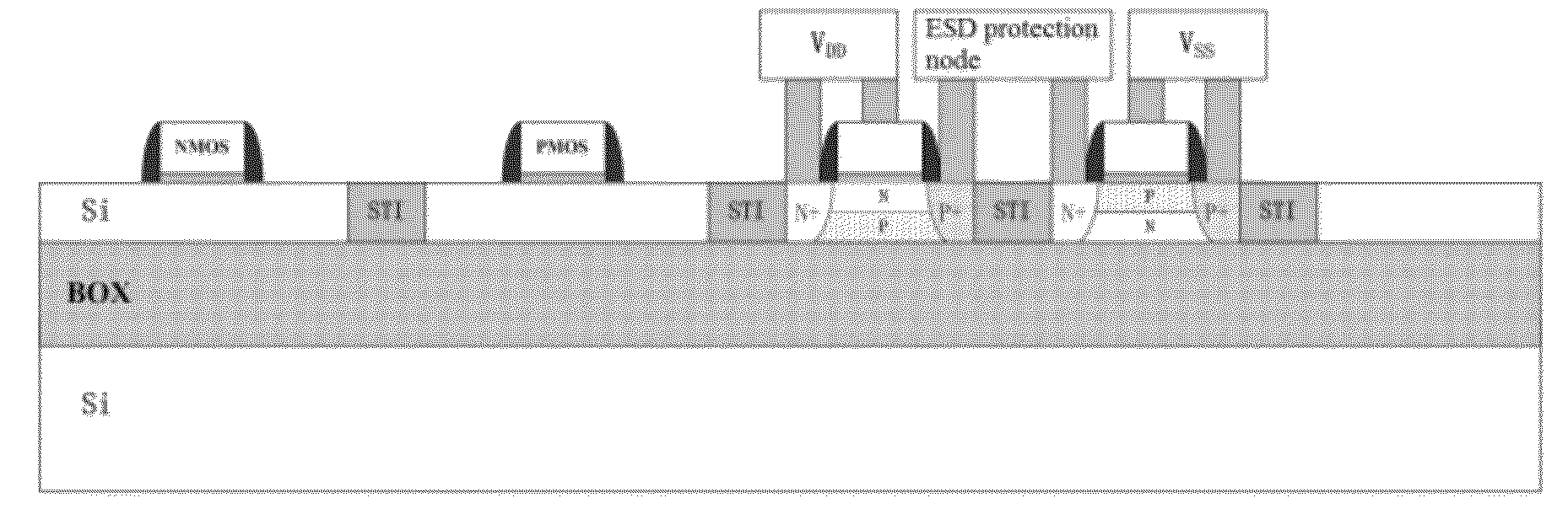
[0022]FIG. 2 illustrates the cross sectional view of a P-type gate-diode ESD protection structure in a SOI circuit, according to the first embodiment of the present disclosure. The P-type gated-diode ESD protection structure in a SOI circuit includes a semiconductor substrate 4 and a P-type gated diode ESD protection device 10 (enclosed in the dashed lined box) formed on the semiconductor substrate 4.
[0023]The semiconductor substrate 4 includes a Si substrate 3; a buried oxide layer (BOX) 2 formed on the Si substrate 3 and a top silicon film 1 formed on the buried oxide layer 2. There are a number of PMOS transistors and NMOS transistors in the vicinity, generally isolated from each other by shallow trench isolation region (STI) 18 fabricated in the semiconductor substrate 4. For reference, only one PMOS transistor 5 and one NMOS transistor 6 are shown in FIG. 2
[0024]The P-type gated diode ESD protection device 10 includes a channel 19, a positive electrode (P+ region) 11, a negativ...
second embodiment
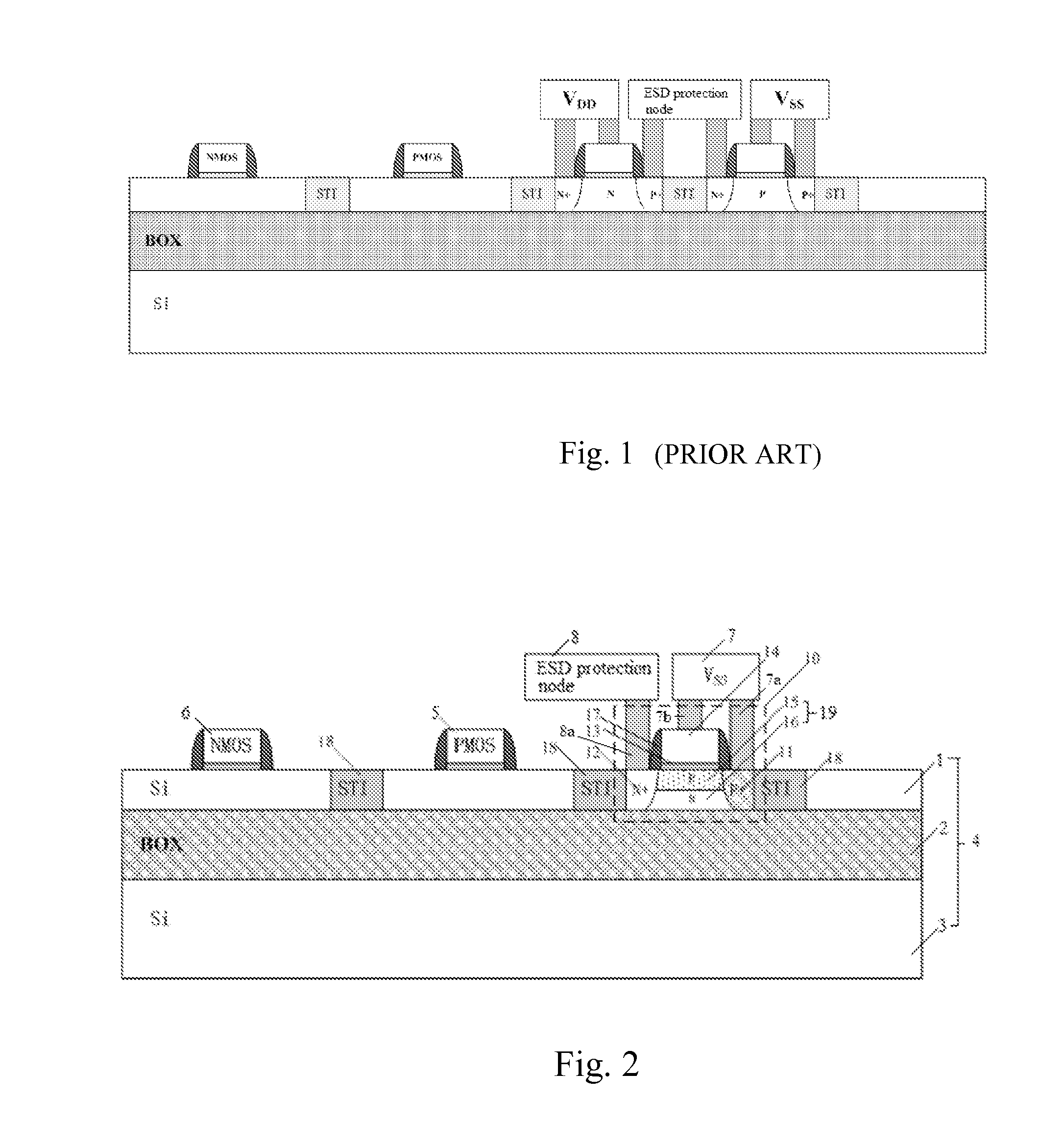
[0028]FIG. 3 is the cross sectional view of an N-type gated single diode ESD protection structure, according to the second embodiment of the present invention. The N-type gated single diode ESD protection structure includes a semiconductor substrate 34, and a N-type gated diode ESD protection device 20 formed on the semiconductor substrate 34; the semiconductor substrate 34 includes a Si substrate 33; a buried oxide layer (BOX) 32 formed on the Si substrate 33, and a top silicon film 31 formed on the buried oxide layer 32. There are a number of PMOS transistors and NMOS transistors in the vicinity, isolated by shallow trench isolation region (STI) 38 fabricated on the semiconductor substrate 34. For reference, only one PMOS transistor 35 and one NMOS transistor 36 are shown in FIG. 3.
[0029]The N-type gated diode ESD protection device 20 includes a channel 29, a positive electrode (P+ region) 21, a negative electrode (N+ region) 22 formed respectively at the two opposite ends of the ...
third embodiment
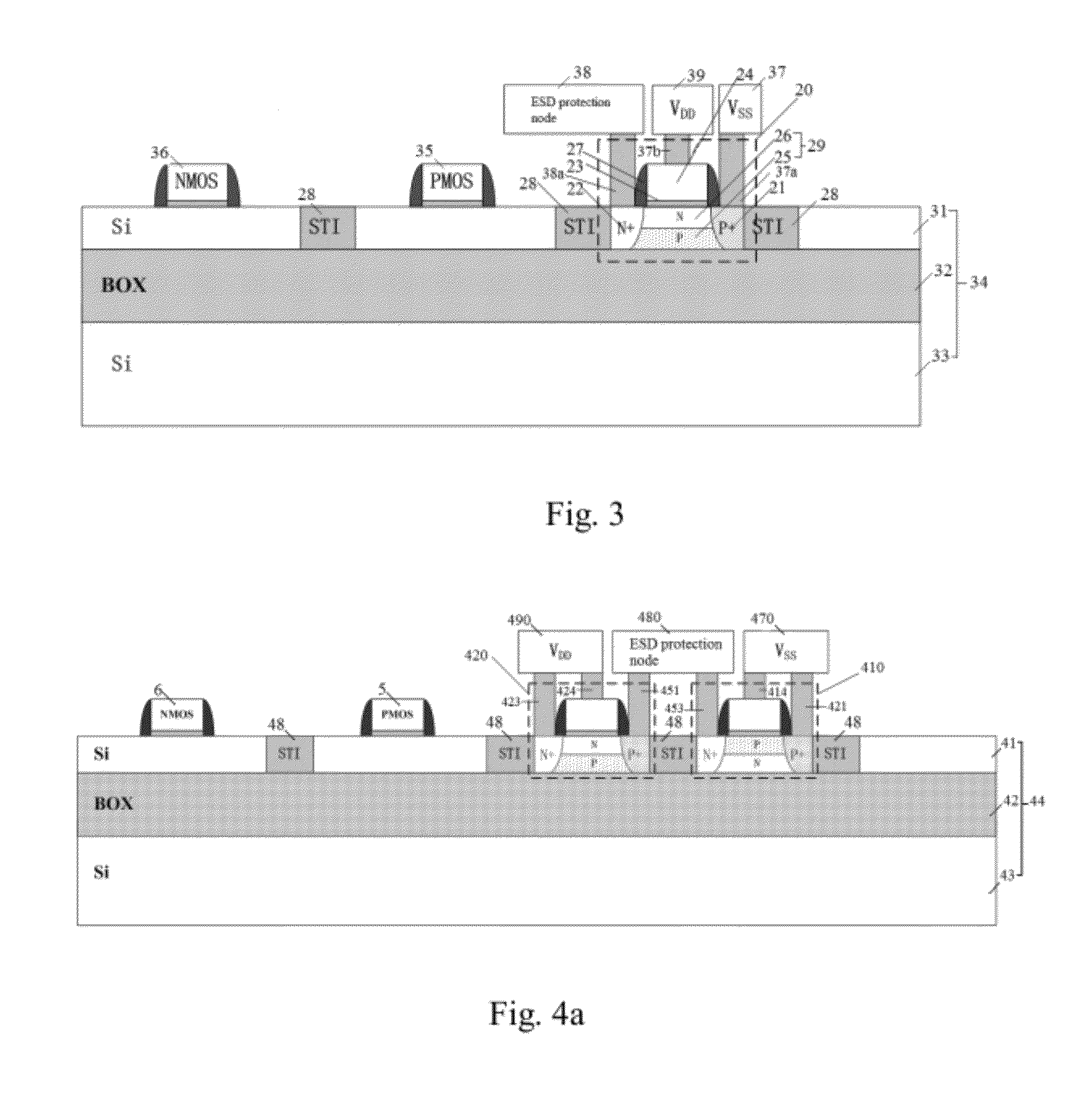
[0033]FIG. 4a is the cross sectional view of a gated duo-diode ESD protection structure in a SOI CMOS circuit. The gated duo-diode ESD protection structure includes a semiconductor substrate 44, a P-type gated diode ESD protection device 410 and an N-type gated diode ESD protection device 420 formed in the semiconductor substrate 44. The semiconductor substrate 44 includes a Si substrate 43; a buried oxide layer (BOX) 42 formed on the Si substrate 43 and a top silicon film 41 formed on the buried oxide layer 42. A number of PMOS transistors and NMOS transistors in SOI CMOS circuits are isolated from each other by shallow trench isolation region (STI) 48, which are fabricated in the semiconductor substrate 44. A PMOS transistor 5 and a NMOS transistor 6 are shown in FIG. 4a.
[0034]The N-type gated diode ESD protection device 420 and the P-type gated diode ESD protection device 410 are serially connected. The negative electrode 423 and the gate electrode 424 of the N-type gated diode ...
PUM
 Abstract
Description
Claims
Application Information
 - R&D Engineer
- R&D Manager
- IP Professional
- Industry Leading Data Capabilities
- Powerful AI technology
- Patent DNA Extraction
Browse by: Latest US Patents, China's latest patents, Technical Efficacy Thesaurus, Application Domain, Technology Topic, Popular Technical Reports.
© 2024 PatSnap. All rights reserved.Legal|Privacy policy|Modern Slavery Act Transparency Statement|Sitemap|About US| Contact US: help@patsnap.com