Wide range charge balancing capacitive-to-digital converter

a capacitive-to-digital converter, wide-range technology, applied in the direction of analog-digital converters, instruments, transmission systems, etc., can solve the problems of impracticality and cost depending on the desired implementation, and achieve the effect of reducing capacitan

Active Publication Date: 2012-05-10
IDT EURO GMBH
View PDF6 Cites 19 Cited by
  • Summary
  • Abstract
  • Description
  • Claims
  • Application Information

AI Technical Summary

Benefits of technology

[0006]In one aspect, the shortcomings of the prior art are overcome and additional advantages are provided through the provision of a charge balancing capacitive-to-digital converter comprising a sensor capacitor, an offset capacitor, a reference capacitor, an integrator circuit, and a demodulation circuit. The sensor capacitor is switched according to a first clock signal of a first clock schedule, and the offset capacitor is switched according to a second clock signal of a second clock schedule, wherein the second clock schedule is of higher frequency than the first clock schedule. The reference capacitor is provided for charge balancing and is switched according to a return signal from an outp

Problems solved by technology

This can be impractical and costly de

Method used


Image

  • Wide range charge balancing capacitive-to-digital converter
  • Wide range charge balancing capacitive-to-digital converter
  • Wide range charge balancing capacitive-to-digital converter

Examples


Embodiment Construction

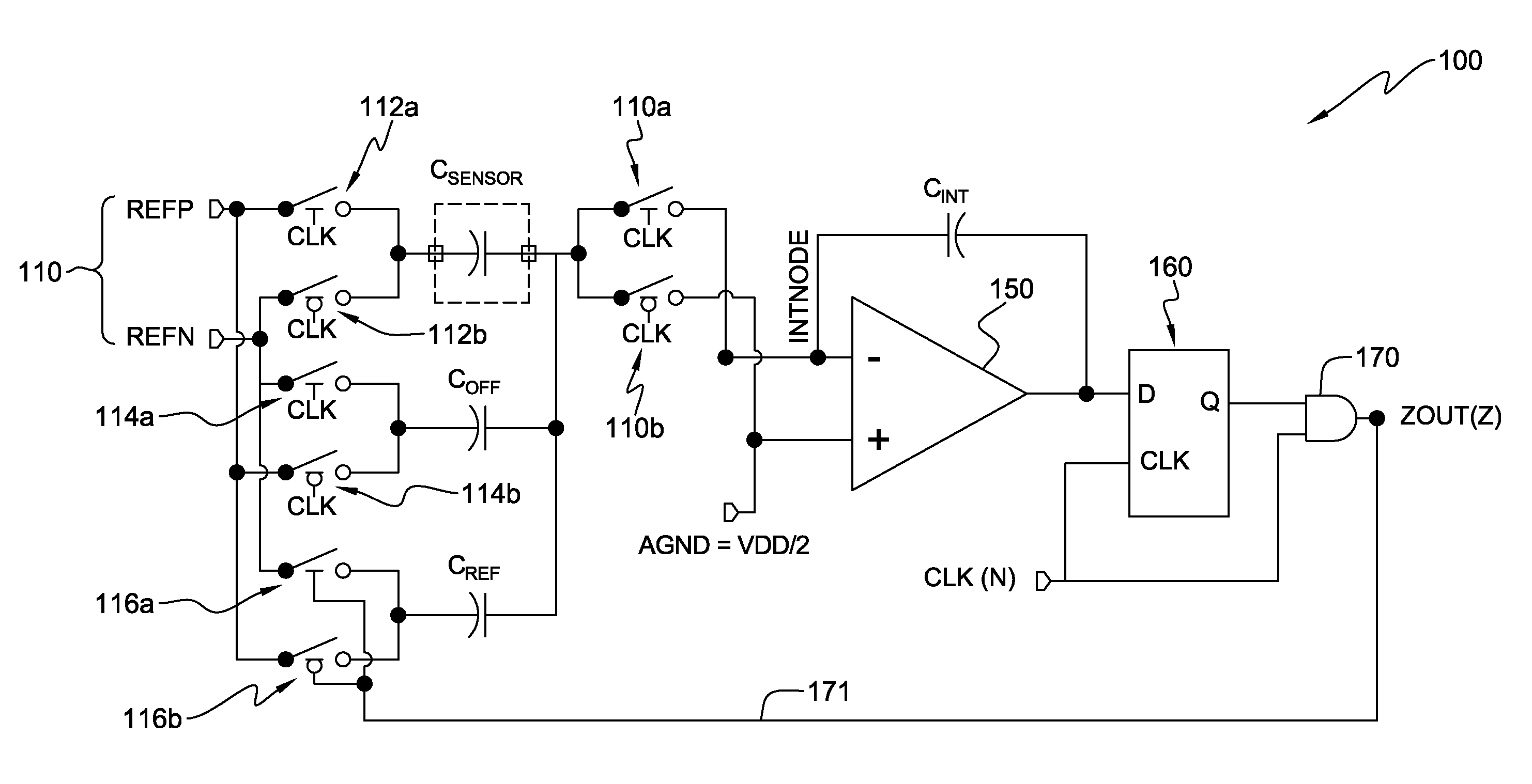
[0014]FIG. 1 shows an example of a charge balancing capacitive-to-digital converter 100. Converter 100 has as a main input CSENSOR whose output node is connected over a first switch 110a to the negative IntNode of an operational amplifier (or integrator) 150 and over a second switch 110b to the positive input of operational amplifier 150. As shown, the first switch is clocked with a clock signal CLK and the second switch with the inverted CLK. The output node of operational amplifier 150 is bridged with the IntNode thereof by an integrator capacitor CINT and is connected via a demodulator 160 to an input of an AND gate 170, which outputs a signal ZOUT (Z). The other input of AND gate 170, as well as the other input of demodulator 160, is connected to receive clock signal CLK (N).

[0015]The input of CSENSOR is connected to REFP over a first switch 112a, which is clocked by CLK, and to REFN over a second switch 112b, clocked by inverted CLK. The difference between REFP and REFN is the ...


PUM


Abstract

A capacitive-to-digital converter is provided which includes: sensor, offset and reference capacitors, an integrator circuit and a demodulation circuit. The sensor capacitor is switched according to a first clock and the offset capacitor according to a second clock, which has a higher switching frequency. The reference capacitor is switched according to a return signal from the converter's output. The integrator circuit includes an integrator capacitor, and has first and second nodes, with the sensor, offset and reference capacitors each being switched to the first and second nodes based on the respective first clock, second clock or return signal. The demodulation circuit receives and converts output of the integrator circuit into a digital output. The higher frequency clocking of the offset capacitor allows for a reduction in capacitance of the offset, reference or integrator capacitor, and the multiclocking of the converter allows for use of a multireferencing to the sensor capacitor.

Description

CROSS-REFERENCE TO RELATED APPLICATION[0001]This application claims the benefit of U.S. Provisional Application No. 61 / 143,851, filed Jan. 12, 2009, which is hereby incorporated herein by reference in its entirety.BACKGROUND[0002]The present invention relates in general to a wide range capacitive-to-digital charge balancing converter based on complementary metal-oxide-semiconductor (CMOS) devices for accurate capacitance-to-digital conversion of a capacitive sensor signal.[0003]Capacitive sensor signal-conditioning integrated circuits, such as the cLite™ capacitive sensor signal conditioner (or cLite™ ASSP (Application Specific Standard Product)) available from Zentrum Mikroelektronik Dresden (ZMD) AG of Dresden Germany, comprise a capacitive-to-digital converter and are able to convert a capacitance within a selectable range (for example, 2-260 pF in the case of the cLite™ signal conditioner) to a corresponding digital value. Advantageously, the cLite™ signal conditioner currently ...

Claims


Application Information

Patent Timeline
IPC IPC(8): H03M1/12
CPCH03M1/60
Inventor KRAUSS, MATHIASJAAFAR, MAHAWANG, KEHOFFMAN, ERIC
Owner IDT EURO GMBH
Why Eureka
Try Eureka