Island matrixed gallium nitride microwave and power switching transistors

a gallium nitride and microwave technology, applied in the field of gallium nitride transistors, can solve the problems of yield loss of older gallium arsenide devices and newer gallium nitride devices, and achieve the effect of reducing surface interconnect and pad requirements, reducing yield loss, and increasing gate width

Active Publication Date: 2012-06-07
GAN SYST
View PDF47 Cites 13 Cited by
  • Summary
  • Abstract
  • Description
  • Claims
  • Application Information

AI Technical Summary

Benefits of technology

[0015]The island topology disclosed herein, preferably triangular or rectangular island structures, provide numerous advantages over the common multi-finger or interdigitated structure. These island topologies result in the specific transistor resistance being less than 70% of those achieved by equivalent-area multi-finger layouts. More significantly, the effective overall device area ratios are 3 to 5 times superior because of the reduced surface interconnect and pad requirements.
[0016]The present invention provides a device with a larger gate width (or “Wg”) within a given active area. In certain exemplary embodiments, the topologies provide a great increase in the current handling capability per unit overall device area, rather than just within the active area. In addition, there is provided a simple process to fabricate extremely capable GaN semiconductor devices.
[0017]Another inventive aspect of this invention relates to the design of the field plates buried within various epitaxial layers. Because the silicon conductive substrate will produce unwanted increases in the capacitance of the active regions, a lightly doped singular, dual or a series of epitaxial layers of intrinsic silicon material (lightly doped) can be grown on the substrate. The thickness of this or these layers can be varied and a buried conductive layer or a series of layers can be inserted to act as buried field plates. Multiple field plates of various sizes and shapes can be introduced. These field plates reduce the peak electric field near the gate edge that is juxtaposed to the drain and therefore increases the maximum voltage that the transistor can withstand. In addition, these field plates can be arranged to provide a very even distribution of the electrical stress between the gate edge and the drain edge. A unique and exceptionally linear or very high voltage device can be constructed. The novel vertical epitaxial silicon based structure can in addition assist with problems related to the mechanical stresses that arise due the disparity between the thermal expansion of silicon and gallium nitride.

Problems solved by technology

Both the older gallium arsenide devices and the newer gallium nitride devices suffer yield losses.

Method used


Image

  • Island matrixed gallium nitride microwave and power switching transistors
  • Island matrixed gallium nitride microwave and power switching transistors
  • Island matrixed gallium nitride microwave and power switching transistors

Examples


Embodiment Construction

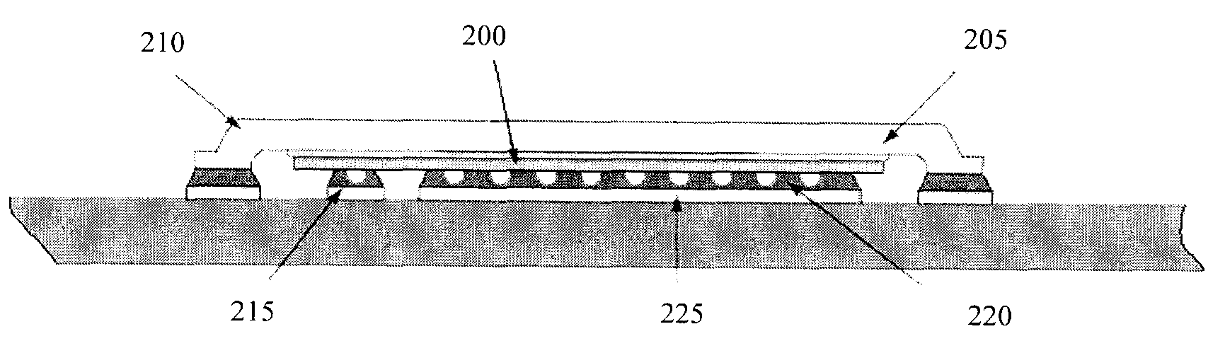
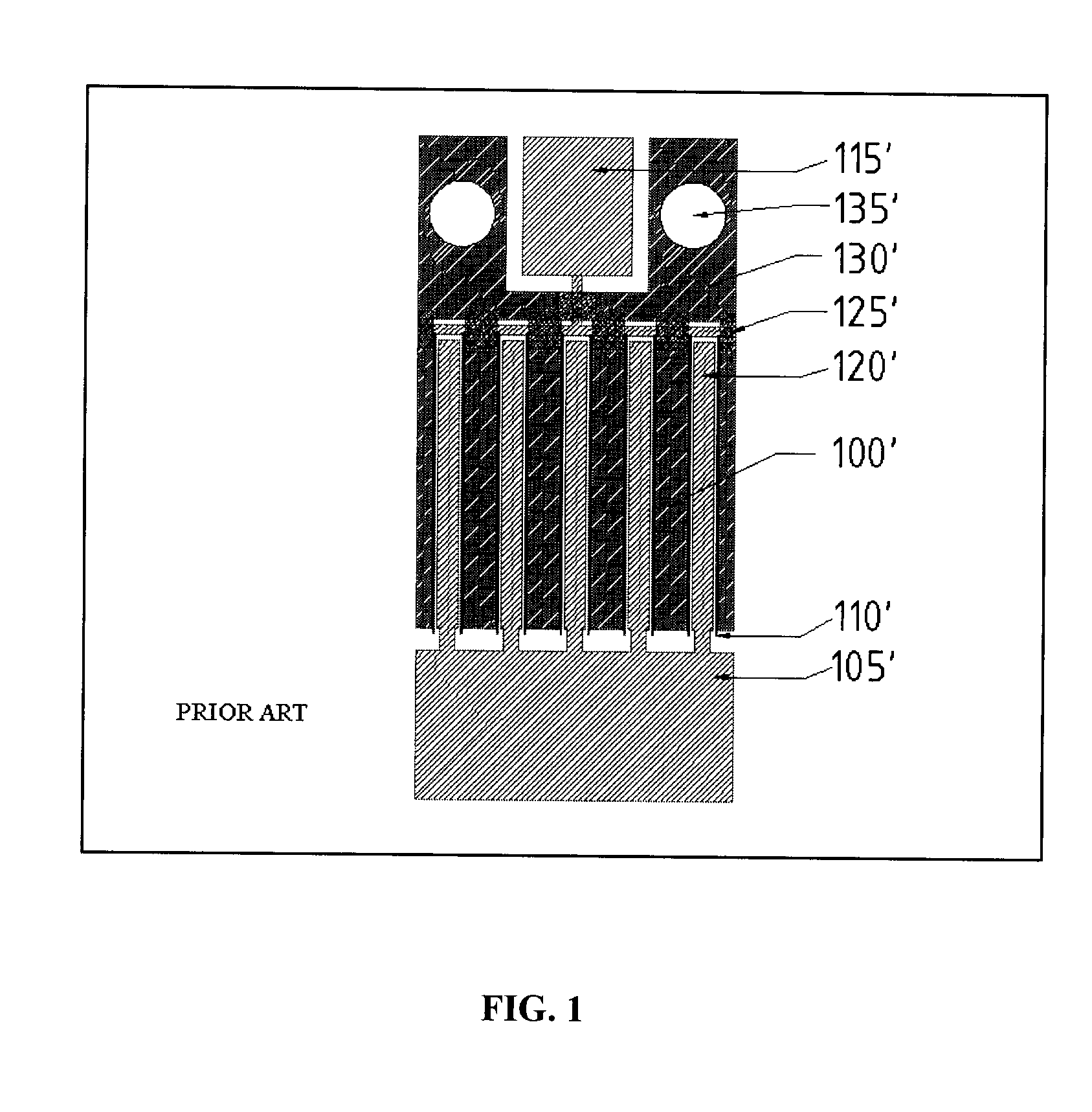
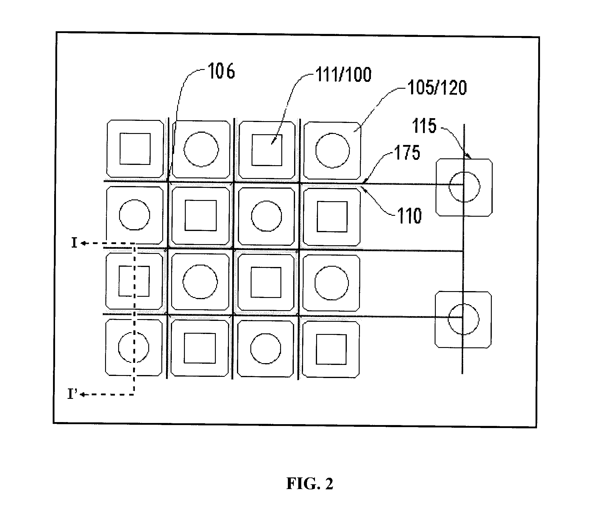
[0028]In the following detailed description of the invention, reference is made to the accompanying drawings that form a part hereof, and in which is shown, by way of illustration, specific embodiments in which the invention may be practiced. In the drawings, like numerals describe substantially similar components throughout the several views. These embodiments are described in sufficient detail to enable those skilled in the art to practice the invention. Other embodiments may be utilized and structural, logical, and electrical changes may be made without departing from the scope of the present invention. The terms wafer template and substrate used in the following description include any structure having an exposed surface with which to form the circuit structure of the invention. The terms substrate or template are understood to include semiconductor wafers. The terms substrate or template are also used to refer to semiconductor structures during processing, and may include other...


PUM


Abstract

A gallium nitride (GaN) device that has greatly superior current handling ability per unit area than previously described GaN devices. The improvement is due to improved layout topology. The layout scheme, which uses island electrodes rather than finger electrodes, is shown to increase the active area density over that of conventional interdigitated structures. Ultra low on resistance transistors can be built using the island topology. Specifically, the present invention, which uses conventional GaN lateral technology and electrode spacing, provides a means to enhance cost/effective performance of all lateral GaN structures.

Description

FIELD OF THE INVENTION[0001]The invention relates generally to gallium nitride transistors and, more particularly, to performance improvement and yield enhancement methods associated with the same.BACKGROUND OF THE INVENTION[0002]Gallium nitride materials include gallium nitride and its alloys such as aluminum gallium nitride, indium gallium nitride and aluminum indium gallium nitride. These materials are semiconductor compounds that have a relatively wide, direct bandgap, which permits highly energetic electronic transitions to occur. Gallium nitride materials have a number of attractive properties including high electron mobility, the ability to efficiently emit blue light and the ability to transmit signals at high frequency, among others. Accordingly, gallium nitride materials are being investigated in many microelectronic applications such as transistors and optoelectronic devices.[0003]Despite the attractive properties noted above, a number of challenges exist in connection wi...

Claims


Application Information

Patent Timeline
Patent Type & Authority Applications(United States)
IPC IPC(8): H01L29/20
CPCH01L29/1075H01L29/2003H01L29/7787H01L29/41758H01L29/42316H01L29/4175H01L2224/73253H01L29/20H01L29/41H01L29/772
Inventor ROBERTS, JOHNMIZAN, AHMADPATTERSON, GIRVANKLOWAK, GREG
Owner GAN SYST
Why Eureka
Try Eureka