Wafer support, chemical vapor phase growth device, epitaxial wafer and manufacturing method thereof

a technology of chemical vapor phase and growth device, which is applied in the direction of polycrystalline material growth, crystal growth process, chemically reactive gas, etc., can solve the problems of uneven surface of epitaxial wafer, increase in and crown interfere with uniform gas supply, so as to achieve effective and sufficient reduction of edge crown and large effective area, the effect of further reducing the width of the edge exclusion zon

Active Publication Date: 2019-02-19
RESONAC CORPORATION
View PDF23 Cites 0 Cited by
  • Summary
  • Abstract
  • Description
  • Claims
  • Application Information

AI Technical Summary

Benefits of technology

[0053]In the wafer support portion according to the present invention, a height from a portion of a reaction space side-upper surface of the wafer support portion, which is most distant from the wafer mounting surface, to a main surface of the wafer mounted on the wafer mounting surface is 1 mm or more. Therefore, the supply of the raw material gas to an outer peripheral portion of the wafer is suppressed, the growth of an edge crown can be suppressed, and an epitaxial wafer having a small width of the edge exclusion zone and a large effective area can be obtained.
[0054]In addition, at least a part of the wafer support includes some of constituent elements of the epitaxial film. Therefore, an element required during the growth of the epitaxial film can be supplied from the wafer support portion, and an epitaxial wafer including the epitaxial film in which a variation in carrier concentration in an in-plane direction is suppressed can be provided.
[0055]The chemical vapor phase growth device according to the present invention includes the above-described wafer support portion. Therefore, by using this chemical vapor phase growth device, an edge crown can be effectively and sufficiently reduced.
[0056]The epitaxial wafer according to the present invention includes the epitaxial film on the main surface of the wafer, in which a height of an edge crown, which is formed on a wafer peripheral portion of the epitaxial film, from a level surface of the epitaxial film is within 30% with respect to a thickness of the epitaxial film at a wafer center. Therefore, the width of the edge exclusion zone can be further reduced, and an epitaxial wafer in which an effective area ratio which can be achieved in a semiconductor chip is high can be achieved.
[0057]In the manufacturing device and the manufacturing method according to the present invention, the above-described wafer support portion is used. Therefore, by using the manufacturing device and the manufacturing method according to the present invention, an edge crown can be effectively and sufficiently reduced, and a SiC epitaxial wafer having a small width of the edge exclusion zone and a large effective area in which the in-plane carrier concentration is uniform can be obtained.

Problems solved by technology

In a manufacturing process of the epitaxial wafer, smoothing a surface of the epitaxial wafer has been an issue for a long time.
For example, in a case where an edge crown is formed on an upstream side of a step flow, this edge crown interferes with uniform gas supply.
Therefore, in an epitaxial film of an epitaxial wafer, defects may occur due to various transfers or the like, and the presence of these defects may also cause an increase in the width of the edge exclusion zone.
In addition, this edge crown may break during transport and damage an epitaxial surface of a wafer, or may cause cracking during processing.

Method used


Image

  • Wafer support, chemical vapor phase growth device, epitaxial wafer and manufacturing method thereof
  • Wafer support, chemical vapor phase growth device, epitaxial wafer and manufacturing method thereof
  • Wafer support, chemical vapor phase growth device, epitaxial wafer and manufacturing method thereof

Examples


example 1

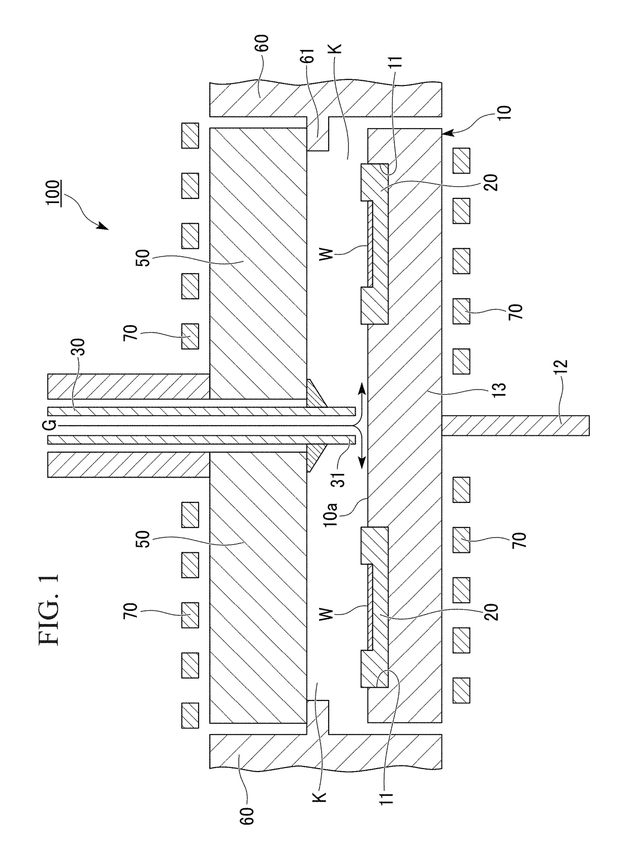
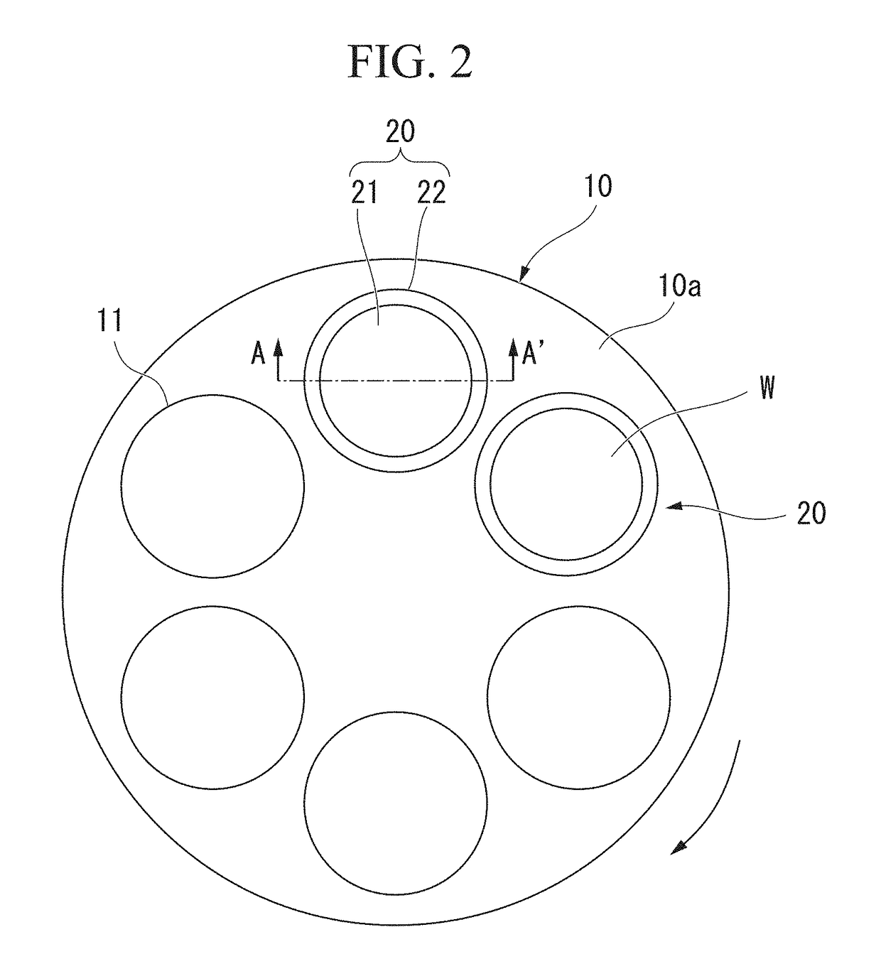
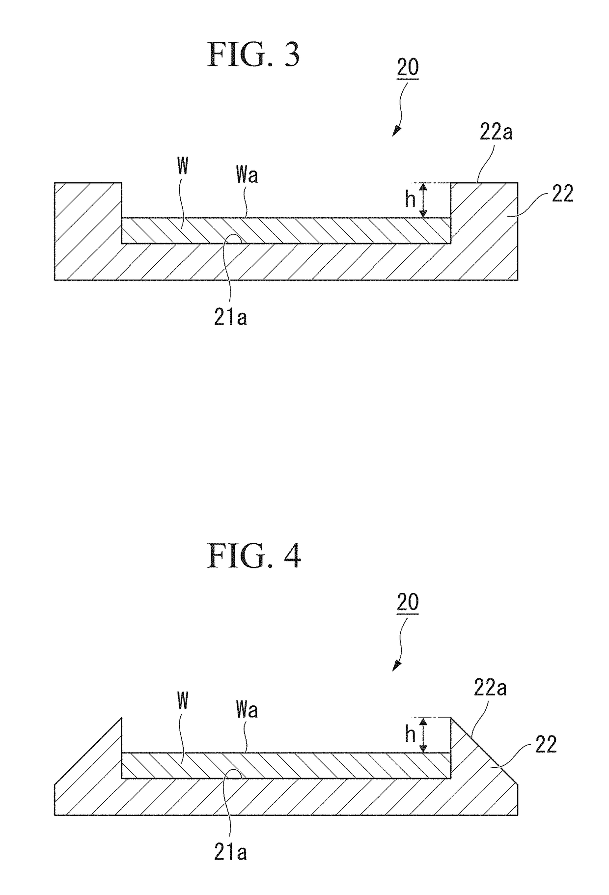
[0181]As a wafer, a 4-inch (0001) Si-face 4° off-axis SiC substrate having a thickness of 350 μm in which an OF is provided was used. This wafer was mounted on a wafer support in a planetary chemical vapor phase growth device. At this time, a ring-shaped member as a wafer support portion was disposed around the wafer. The thickness of the ring-shaped member was 2 mm. A cross-section of the ring-shaped member was quadrangular, and a height from a reaction space side-upper surface of the ring-shaped member to a main surface of the wafer mounted on the wafer mounting surface was 1.65 mm. In the ring-shaped member, a linear portion was provided at a position corresponding to the OF portion of the wafer such that the inside of the ring-shaped member is disposed along the periphery of the wafer. The distance between the wafer periphery and the ring-shaped member was 0.15 μm.

[0182]As a raw material gas, a mixed gas of silane and propane was used, hydrogen gas was used as a carrier gas, and...

example 2

[0184]The thickness of the edge crown was measured under the same conditions as those in Example 1, except that the internal shape of the ring-shaped member was circular and an OF portion was not provided.

[0185]As a result, the height of the edge crown formed on the OF surface of the SiC substrate was 24 μm, and the height of the edge crown in an outer peripheral surface other than the OF surface was 8 μm.

example 3

[0186]The thickness of the edge crown was measured under the same conditions as those in Example 2, except that a SiC substrate having a thickness of 500 μm was used as the wafer.

[0187]As a result, the height of the edge crown formed on the OF surface of the SiC substrate was 32 μm, and the thickness of the edge crown in an outer peripheral surface other than the OF surface was 9 μm.


PUM

PropertyMeasurementUnit
temperatureaaaaaaaaaa
pressureaaaaaaaaaa
thicknessaaaaaaaaaa

Abstract

Provided is a manufacturing device capable of effectively and sufficiently reducing an edge crown. The wafer support is used in a chemical vapor phase growth device in which an epitaxial film is grown on a main surface of a wafer using a chemical vapor deposition method, the wafer support including: a wafer mounting surface having an upper surface on which a substrate is mounted; and a wafer support portion that rises to surround a wafer to be mounted, in which a height from an apex of the wafer support portion to a main surface of the wafer mounted on the wafer mounting surface is 1 mm or more.

Description

CROSS REFERENCE TO RELATED APPLICATIONS[0001]This application is a National Stage of International Application No. PCT / JP2015 / 083377 filed Nov. 27, 2015, claiming priority based on Japanese Patent Application No. 2014-243939, filed Dec. 2, 2014 and Japanese Patent Application No. 2014-257833, filed Dec. 19, 2014, the contents of all of which are incorporated herein by reference in their entirety.TECHNICAL FIELD[0002]The present invention relates to a wafer support, a chemical vapor phase growth device, an epitaxial wafer, and a manufacturing method thereof.[0003]Priority is claimed on Japanese Patent Application No. 2014-243939, filed Dec. 2, 2014 and Japanese Patent Application No. 2014-257833, filed Dec. 19, 2014, the contents of which are incorporated herein by reference.BACKGROUND ART[0004]As means for forming a thin film on a substrate, for example, various film forming methods such as a sputtering method, a vacuum deposition method, or a chemical vapor deposition (CVD) method ...

Claims


Application Information

Patent Timeline
Patent Type & Authority Patents(United States)
IPC IPC(8): H01L21/02H01L21/687C23C16/455C30B25/16H01L29/16C30B29/36C23C16/32C23C16/458C30B25/12C30B25/20
CPCC30B25/20C23C16/4581C23C16/4584C23C16/4585C23C16/45504C30B25/12C30B25/165C30B29/36H01L21/0262H01L21/02378H01L21/02433H01L21/02529H01L21/68721H01L21/68735H01L21/68764H01L21/68771H01L29/1608C23C16/325H01L21/02634
Inventor MUTO, DAISUKENORIMATSU, JUN
Owner RESONAC CORPORATION
Why Eureka
Try Eureka