Optical receiver with monolithically integrated photodetector

a monolithic integrated, optical receiver technology, applied in the field of optical receivers, can solve the problems of extra overhead and assembly cost of the photodetector, and achieve the effect of increasing bandwidth and phase margin

Inactive Publication Date: 2012-06-07
THE GOVERNING COUNCIL OF THE UNIV OF TORONTO
View PDF4 Cites 43 Cited by
  • Summary
  • Abstract
  • Description
  • Claims
  • Application Information

AI Technical Summary

Benefits of technology

[0014]The amplifier may comprise a negative Miller capacitor incorporated into a core of the amplifier to extend an internal pole of the amplifier for increased bandwidth and phase margin.

Problems solved by technology

Although this solution allows for the use of high quality and high data rate photodetectors, extra overhead and assembly cost associated with the photodetector, as well as electrostatic discharge (ESD) problems and other parasitics associated with the bond wires, may be some of the resulting drawbacks.

Method used


Image

  • Optical receiver with monolithically integrated photodetector
  • Optical receiver with monolithically integrated photodetector
  • Optical receiver with monolithically integrated photodetector

Examples


Embodiment Construction

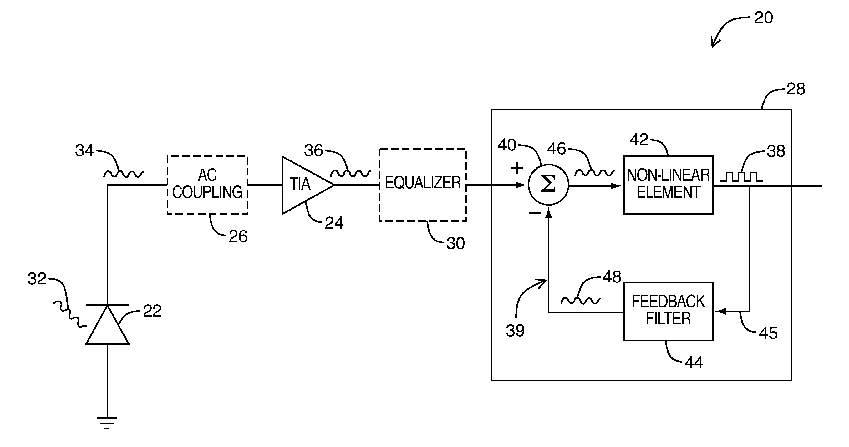
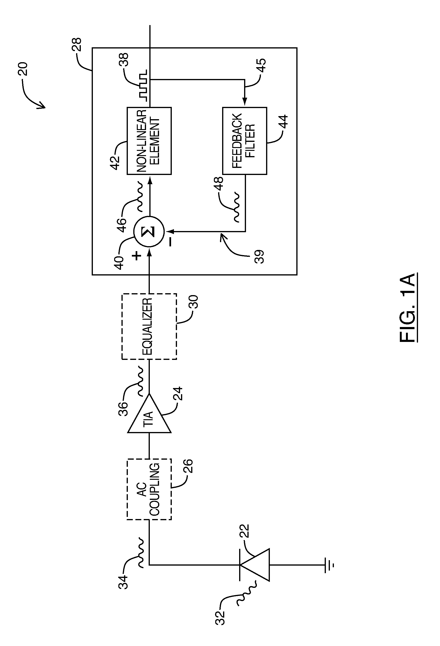
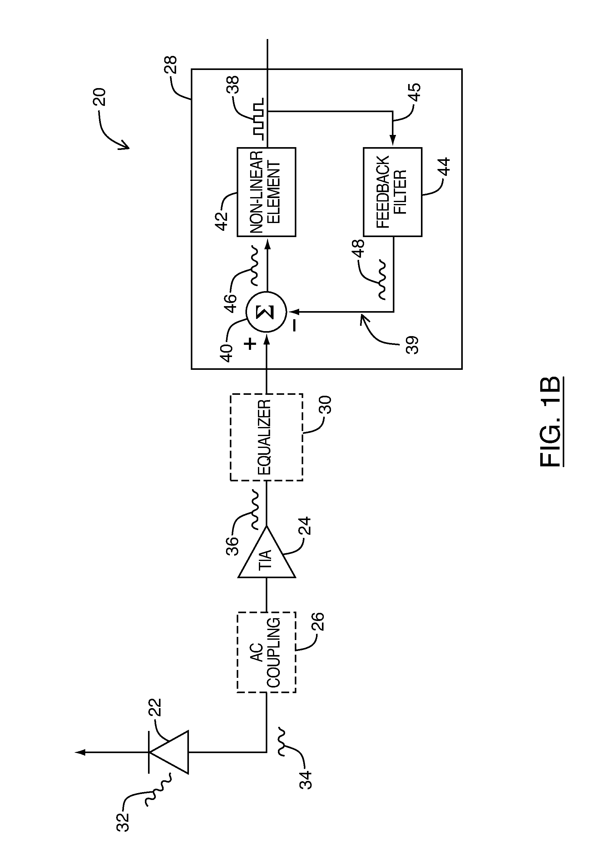
[0044]Although CMOS and other integrated photodetectors may conveniently minimize use of bond wires and reduce overhead, these types of photodetectors tend to generate significantly distorted detection signals due to their particular mechanisms of detection. Most light photons incident on the photodetector are absorbed either in the depletion region of the photodetector or deep into the underlying substrate depending on the penetration depth of the photon. Charge carriers generated within the depletion region are transported to the photodetector terminals relatively quickly through carrier drift in the presence of the reverse biased electric field applied to the pn junction. However, those charge carriers generated deep in the underlying substrate are transported initially through carrier diffusion until the charge carriers reach the depletion region, after which point carrier drift again becomes the dominant mode of charge carrier transport to the given photodetector terminal. Comp...


PUM


Abstract

An optical receiver includes a photodetector for detecting incoming optical data signals and an amplifier for providing signal gain and current to voltage conversion. The detection signal generated by the photodetector may include a distortion component caused by an operating characteristic of the photodetector. A signal compensating circuit may reconstruct the received optical data signal by effectively canceling the distortion component. For this purpose, the signal compensating circuit may include a decision feedback equalizer implemented using at least one feedback filter matched to the operating characteristic of the photodetector causing the signal distortion so as to reproduce the distortion component for cancellation. Use of a control module may also configure the optical receiver in real time to account for other operating and environmental conditions of the optical receiver. Data rates in excess of 5 Gbps may be realized in monolithic CMOS photodetectors when the signal compensating circuit is properly matched.

Description

CROSS-REFERENCE TO RELATED APPLICATIONS[0001]This application claims the benefit of U.S. Provisional Application Ser. No. 61 / 351,496 filed on Jun. 4, 2010, the entire contents of which are hereby incorporated by reference.FIELD[0002]Embodiments of the present invention relate generally to optical receivers and, more particularly, to compensated optical receivers having monolithically integrated photodetectors.INTRODUCTION[0003]Optical receivers may be utilized in various different applications, such as local-area networks (LAN) and fiber-to-the-home (FTTH) interconnects, as well as in interfaces for optical storage systems, such as CD-ROM, DVD and Blu-Ray Disc. In these applications, a photodetector may be used to convert incoming optical data signals into electrical detection signals for further processing, such as decoding, amplification, equalization, and compensation. In some types of optical data systems, the photodetector may be housed in a separate chip or as a standalone com...

Claims


Application Information

Patent Timeline
Patent Type & Authority Applications(United States)
IPC IPC(8): H04B10/08
CPCH04B10/6971
Inventor CARUSONE, ANTHONY CHANKAO, TONY SHUO-CHUNYASOTHARAN, HEMESH
Owner THE GOVERNING COUNCIL OF THE UNIV OF TORONTO
Why Eureka
Try Eureka