Lithography system and method of refracting

Active Publication Date: 2012-06-14
ASML NETHERLANDS BV
View PDF8 Cites 20 Cited by
  • Summary
  • Abstract
  • Description
  • Claims
  • Application Information

AI Technical Summary

Benefits of technology

[0015]By applying an electric field between the first electrode and the second electrode, which is embodied as an aperture array, it becomes possible to significantly reduce aberrations introduced by the collimation of the electron beam. By having the electric field from the first electrode terminate at a specific charge on a conductor placed in the beam, the level of reduction of aberrations that can be achieved is much higher than otherwise would be possible by mere adjustment of the voltages and geometry of the converging means. This in turn allows the field size of the exposure to be increased to the required levels.
[0021]In a further embodiment the aperture free areas are provided with conduits for a cooling medium. The use of cooling within the non-beam areas may improve the performance of the exposure tool.
[0029]It has been noticed that not in all cases the aberrations are reduced to the required levels. In a further embodiment the aperture array element is provided with a curved surface. In this manner, aberrations resulting from the electrodes can be reduced.

Problems solved by technology

For high resolution lithography systems designed to operate at a commercially acceptable throughput, the size, complexity, and cost of such systems becomes an obstacle.
An unwanted effect of this increase is that due to the higher current the interactions between the charged particles will increase leading to loss of resolution.
Errors in the projection system will deteriorate the projected image.
Throughout the charged particle optical system many factors contribute to errors in the pattern.
It is a known problem with this type of lens that it suffers from spherical and chromatic aberrations, introduced by the electrodes of the lens, reducing the quality of the projected images.
When increasing the field size of the exposure, these aberrations only increase.
As such the known lenses typically allow for some control of aberrations or beam uniformity, however these cannot provide both requirements to the level required by high-end charged particle lithography.
The known designs cannot reliably and cost effectively provide the reduction in critical dimensions, as required by the roadmap for future development of the lithography industry.
This is not possible with the known designs.

Method used


Image

  • Lithography system and method of refracting
  • Lithography system and method of refracting
  • Lithography system and method of refracting

Examples


first embodiment

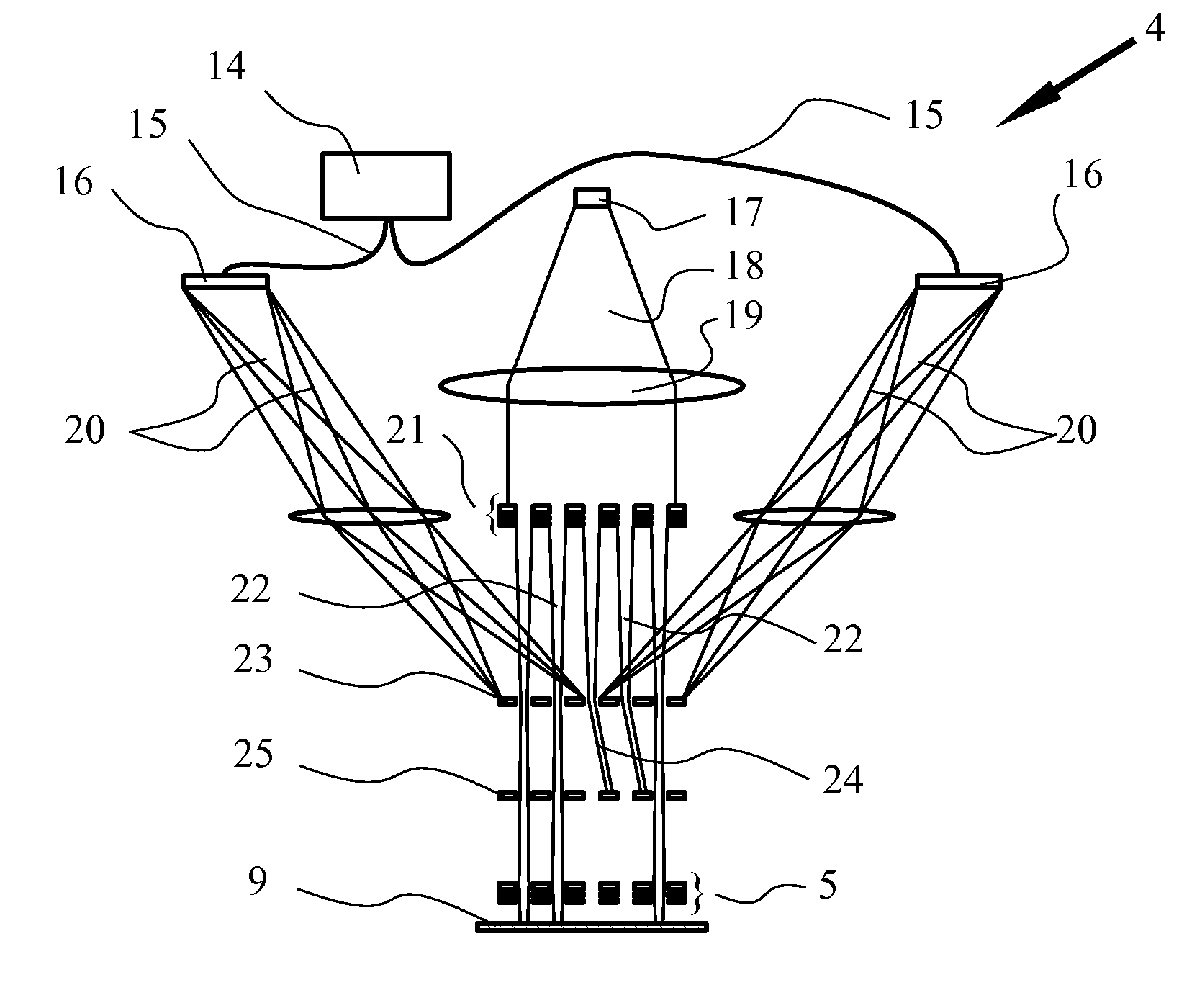
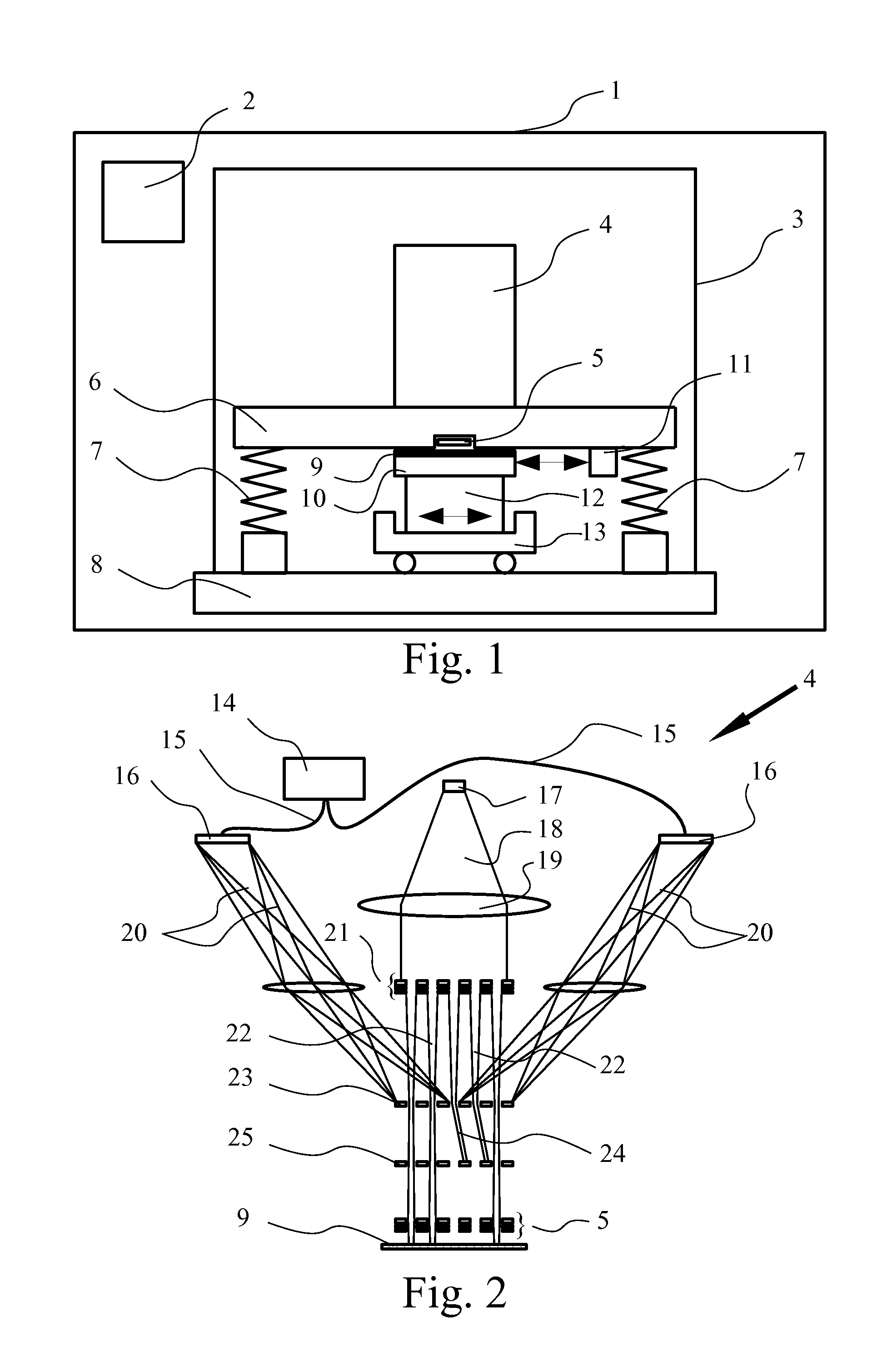
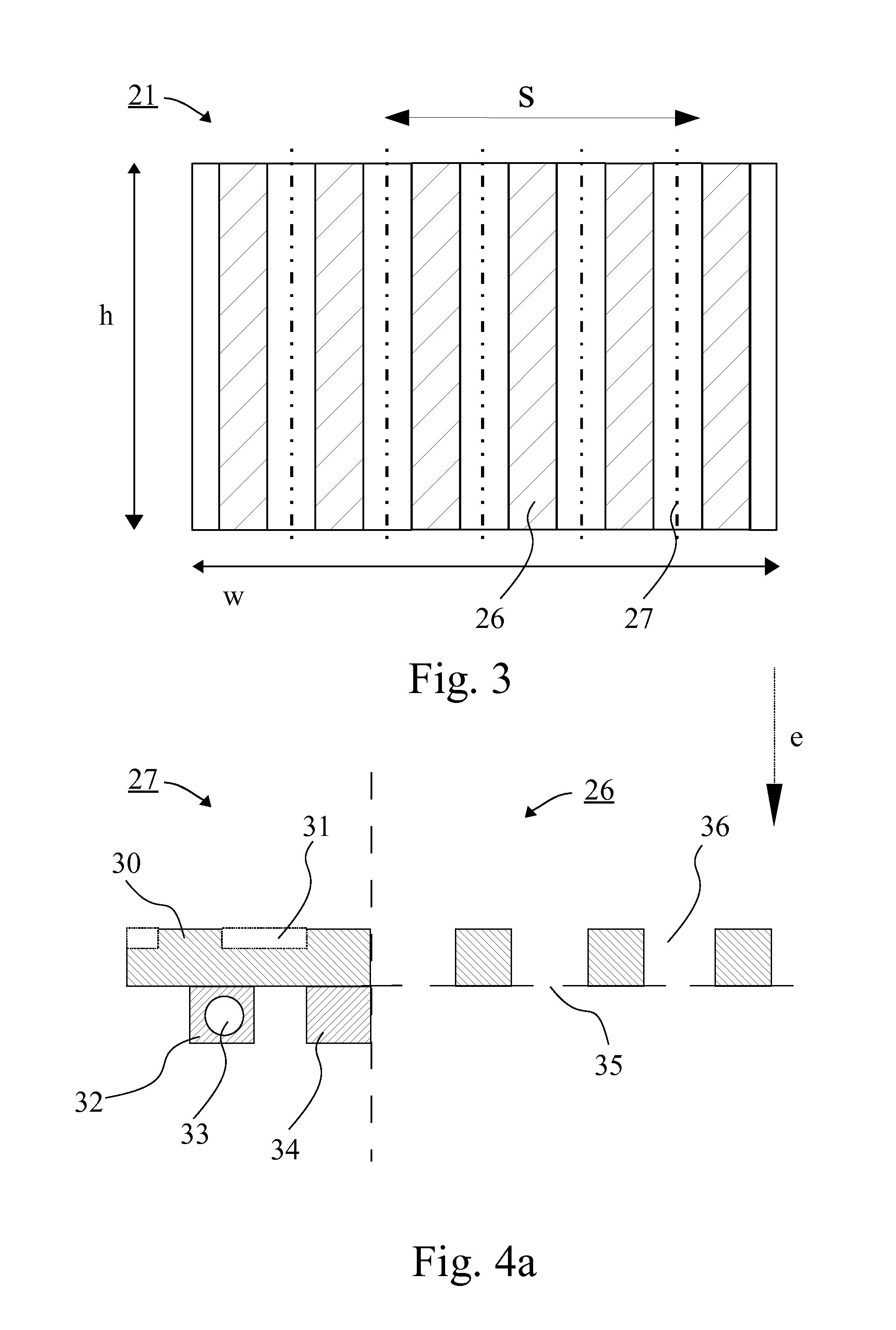
[0062]FIG. 4a schematically shows a cross-section of the aperture array, specifically the transition area between an aperture area 26 and aperture free area 27. In this figure, the direction of the charged particle beam and the direction of the accelerating electric field are indicated by arrow e. While only part of the aperture area 26 and aperture free area 27 is shown, both areas extend in the same plane, and multiple beam and non-aperture areas may be present as shown in FIG. 3. In this embodiment, the second electrode comprises a body 30 in which blind holes 31 are present, which blind holes are equal to the size of the apertures 36. These blind holes serve to preserve the uniformity of the electric field over the transition from aperture area to non aperture area. By maintaining the uniformity of the electric field, the charged particle beam is not disrupted right at the transition from aperture area to non aperture area.

[0063]The electrode may comprise support struts 32, 34 i...

second embodiment

[0065]FIG. 4b schematically shows a cross section of the aperture array, where the aperture array is effectively raised above the surface of the body. It was found that creating one large blind hole 40 in the aperture free area 27, effectively raising the upper surface of the aperture area 26 above the upper surface of the aperture free area (in a direction facing the source, from which the beamlets arrive at the aperture array) also helps to preserve the uniformity of the electric field. Advantageously, this reduces the complexity of the aperture free area thus easing manufacture and reducing cost.

[0066]In the embodiments according to FIGS. 4a and 4b, the current limiting apertures may be recessed below the upper surface of the aperture area 26 facing the source. The recesses may be made by forming the apertures with a larger diameter entry (where beams enter the aperture) and smaller diameter current limiting portion part way along the bore of the aperture or at the exit (where th...


PUM


Abstract

A charged particle lithography system for transferring a pattern onto the surface of a target, such as a wafer, comprising a charged particle source adapted for generating a diverging charged particle beam, a converging means for refracting said diverging charged particle beam, the converging means comprising a first electrode, and an aperture array element comprising a plurality of apertures, the aperture array element forming a second electrode, wherein the system is adapted for creating an electric field between the first electrode and the second electrode.

Description

BACKGROUND OF THE INVENTION[0001]1. Field of the Invention[0002]The present invention relates to an imaging system and in particular to a charged particle multi-beamlet lithography system or inspection system.[0003]2. Description of the Related Art[0004]Currently, most commercial lithography systems use a mask as a means to store and reproduce the pattern data for exposing a target, such as a wafer with a coating of resist. In a maskless lithography system, beamlets of charged particles are used to write the pattern data onto the target. The beamlets are individually controlled, for example by individually switching them on and off, to generate the required pattern. For high resolution lithography systems designed to operate at a commercially acceptable throughput, the size, complexity, and cost of such systems becomes an obstacle.[0005]Furthermore, existing charged particle beam technology is suitable for lithography systems for relatively course patterning of images, for example t...

Claims


Application Information

Patent Timeline
IPC IPC(8): H01J3/14
CPCH01J37/09H01J2237/002H01J2237/31774H01J2237/1534H01J2237/0453
Inventor VAN VEEN, ALEXANDER HENDRIK VINCENTZHANG, YANXIABERGLUND, GUN SARI MARIKRUIT, PIETER
Owner ASML NETHERLANDS BV
Why Eureka
Try Eureka