Oxide thin film transistor and method of fabricating the same

Active Publication Date: 2012-06-14
LG DISPLAY CO LTD
View PDF1 Cites 11 Cited by
  • Summary
  • Abstract
  • Description
  • Claims
  • Application Information

AI Technical Summary

Benefits of technology

[0045]In the method for fabricating an oxide thin film transistor according to an embodiment of the invention, since the amorphous oxide semiconductor is used as the active layer, excellent uniformity can be obtained and the oxide thin film transistor can be applicable to a large scale display.
[0046]In this instance, the amorphous oxide semiconductor reacts to plasma in a follow-up process, changing the carrier concentration of the channel region, but in the method for fabricating an oxide thin film transistor according to an embodiment of the invention, the change in the carrier

Problems solved by technology

The above-described LCD is a display device which has come into prominence so far with its advantages of being light and consuming a small amount of power, but it is a light receiving device, not a light emitting device, and has a technical limitation with respect to brightness, a contrast ratio, a viewing angle, and the like.
The amorphous silicon thin film transistor used for the above-described LCD may be fabricated in a low temperature process, but has a very small mobility and does not satisfy constant current bias conditions.
Meanwhile, a polycrystalline silicon thin film transistor has high mobility and satisfies the consta

Method used


Image

  • Oxide thin film transistor and method of fabricating the same
  • Oxide thin film transistor and method of fabricating the same
  • Oxide thin film transistor and method of fabricating the same

Examples


Example

[0062]An oxide thin film transistor (TFT) according to embodiments of the invention will now be described in detail with reference to the accompanying drawings.

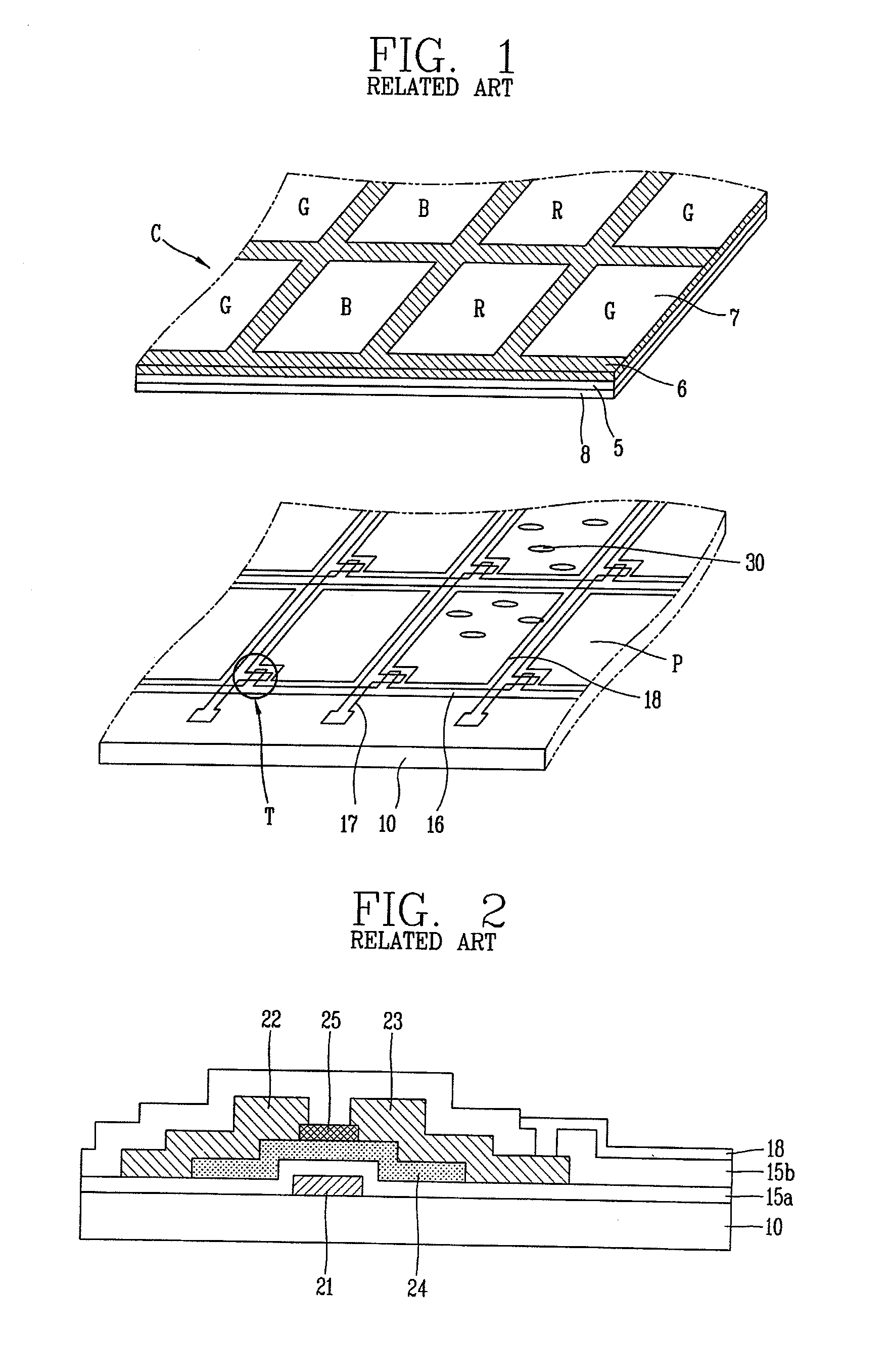
[0063]FIG. 4 is a plan view showing a portion of an array substrate of a liquid crystal display (LCD) device according to an embodiment of the invention. In actuality, N number of gate lines and M number of data lines are formed to cross each other to define the M×N number of pixels in the LCD device, but in order to simplify the explanation, only a single pixel is shown in FIG. 4.

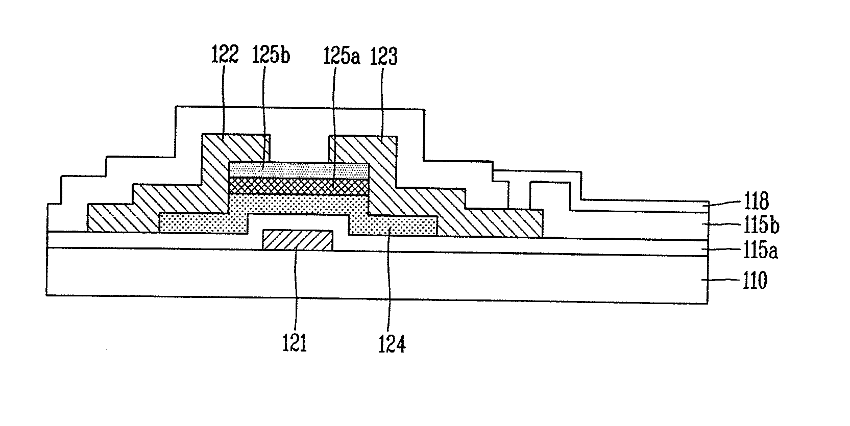
[0064]FIG. 5 is a sectional view schematically showing a structure of an oxide thin film transistor (TFT) according to an embodiment of the invention, which is taken along line A-A′ of the array substrate illustrated in FIG. 4. In this instance, FIG. 5 schematically shows the structure of an oxide TFT using a ternary system or quaternary system oxide semiconductor comprising a combination of AxByCzO (A, B, C═Zn, Cd, Ga, In, Sn, Hf, Zr; x, y, z≧0), a...


PUM


Abstract

A method for fabricating an oxide thin film transistor includes sequentially forming a gate insulating film, an oxide semiconductor layer, and a first insulating layer; selectively patterning the oxide semiconductor layer and the first insulating layer to form an active layer and an insulating layer pattern on the gate electrode; forming a second insulating layer on the substrate having the active layer and the insulating layer pattern formed thereon; and selectively patterning the insulating layer pattern and the second insulating layer to form first and second etch stoppers on the active layer. The oxide semiconductor layer may be a ternary system or quaternary system oxide semiconductor comprising a combination of AxByCzO (A, B, C═Zn, Cd, Ga, In, Sn, Hf, Zr; x, y, z≧0).

Description

CROSS-REFERENCE TO RELATED APPLICATION[0001]This application claims priority to and the benefit of Korean Patent Application No. 10-2010-0127171, filed on Dec. 13, 2010, which is hereby incorporated by reference.BACKGROUND OF THE INVENTION[0002]1. Field of the Invention[0003]Embodiments of invention relate to a method for fabricating an oxide thin film transistor, and more particularly, to a method for fabricating an oxide thin film transistor using a ternary system or quaternary system oxide semiconductor comprising a combination of AxByCzO (A, B, C═Zn, Cd, Ga, In, Sn, Hf, Zr; x, y, z≧0) as an active layer.[0004]2. Description of the Related Art[0005]As interest in information displays is growing and demand for portable (mobile) information medium is increasing, research and commercialization of lighter and thinner flat panel displays (“FPD”), which may substitute for cathode ray tubes (CRTs), the theretofore conventional display devices, have been actively ongoing. Among FPDs, the...

Claims


Application Information

Patent Timeline
IPC IPC(8): H01L33/08H01L21/34
CPCH01L29/7869H01L27/1225
Inventor KIM, DAE-HWANCHOI, BYUNG-KOOKLEE, SULYIM, HOON
Owner LG DISPLAY CO LTD
Why Eureka
Try Eureka