Packaging substrate having through-holed interposer embedded therein and fabrication method thereof

Active Publication Date: 2012-06-14
UNIMICRON TECH CORP
View PDF2 Cites 113 Cited by
  • Summary
  • Abstract
  • Description
  • Claims
  • Application Information

AI Technical Summary

Benefits of technology

[0022]Therefore, by embedding a through-holed interposer in a molding layer, the present invention avoids stacking of the through-holed interposer on a packaging substrate so as to reduce the thickness of the overall structure. Further, by forming a built-up structure on the second surface of the molding layer, the present invention eliminates the need of a core board so as to further reduce the thic

Problems solved by technology

However, the low-k dielectric material is porous and fragile such that in thermal cycling reliability testing after the flip-chip packaging process, a large CTE (Coefficient of Thermal Expansion) difference between the packaging substrate 10 and the semiconductor chip 12 causes an uneven thermal stress on the solder bumps 11, thereby easily resulting in cracking of the solder bumps 11 and even cracking of the semiconductor chip 12.
As such, the product yield and reliability are decreased.
On the other hand, pitches between the flip-chip solder pads 100 of the conventional packaging substrate 10

Method used


Image

  • Packaging substrate having through-holed interposer embedded therein and fabrication method thereof
  • Packaging substrate having through-holed interposer embedded therein and fabrication method thereof
  • Packaging substrate having through-holed interposer embedded therein and fabrication method thereof

Examples


Embodiment Construction

[0032]The following illustrative embodiments are provided to illustrate the disclosure of the present invention, these and other advantages and effects can be apparent to those in the art after reading this specification.

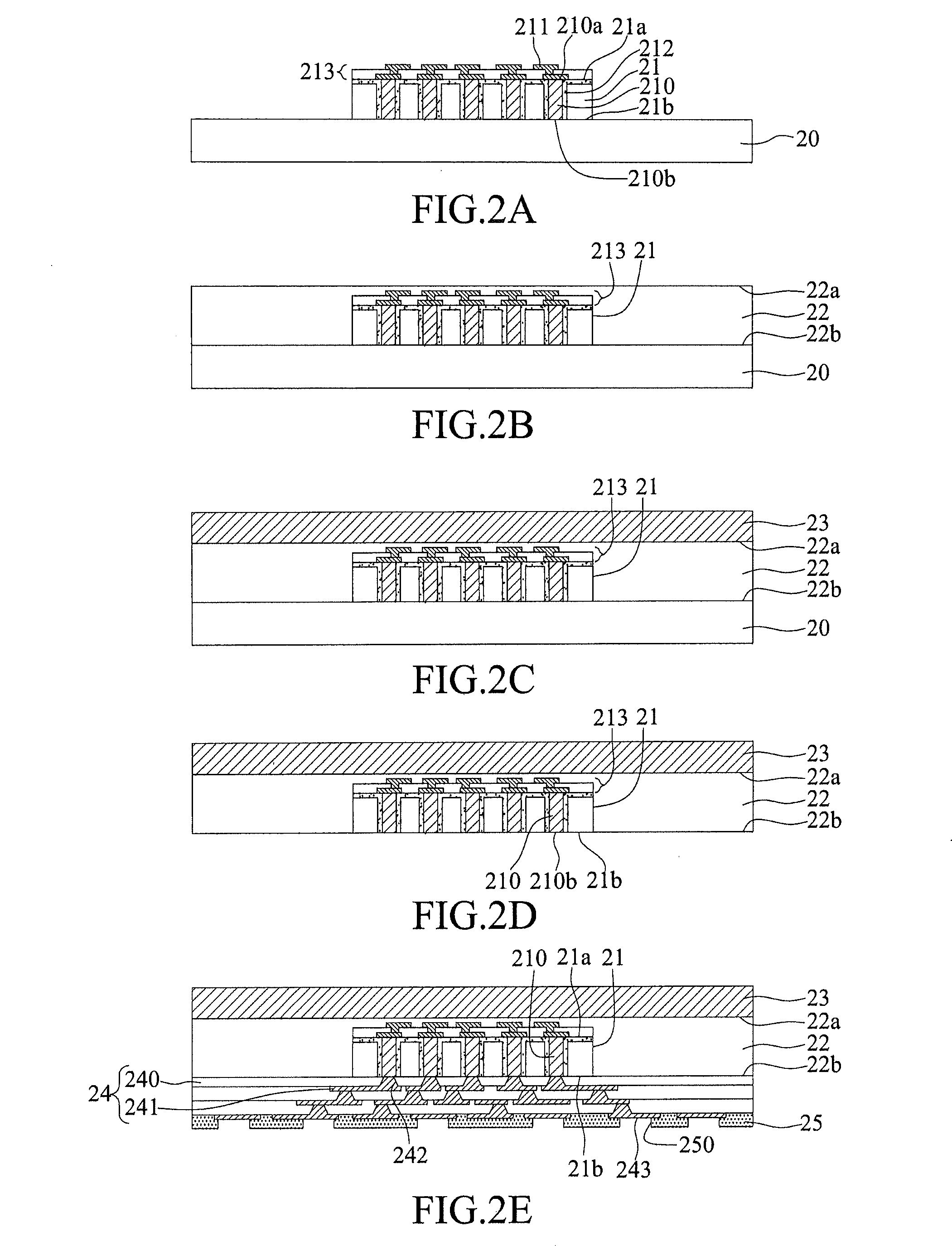
[0033]FIGS. 2A to 2F are cross-sectional views showing a fabrication method of a packaging substrate having a through-holed interposer embedded therein according to the present invention.

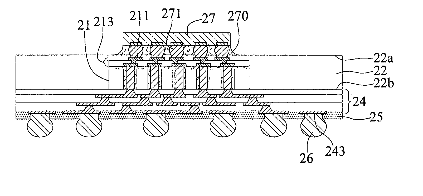
[0034]Referring to FIG. 2A, a carrier board 20 and a through-holed interposer 21 having a redistribution-layer 213 disposed thereon are provided.

[0035]The through-holed interposer 21 has a first side 21a, an opposite second side 21b, and a plurality of conductive through holes 210 penetrating the first side 21a and the second side 21b. Each of the conductive through holes 210 has a first end surface 210a on the first side 21a and a second end surface 210b on the second side 21b, and the second end surface 210b is flush with the second side 21b so as to allow the second side 21b and ...


PUM


Abstract

A packaging substrate having a through-holed interposer embedded therein is provided, which includes: a molding layer having opposite first and second surfaces; a through-holed interposer embedded in the molding layer and flush with the second surface; a redistribution-layer structure embedded in the molding layer and disposed on the through-holed interposer and having a plurality of electrode pads exposed from the first surface of the molding layer; and a built-up structure disposed on the second surface of the molding layer and electrically connected to the through-holed interposer. By embedding the through-holed interposer in the molding layer and forming the built-up structure on the second surface of the molding layer, the present invention eliminates the need of a core board and reduces the thickness of the overall structure. Further, since the through-holed interposer has a CIE close to or the same as that of a silicon wafer, the structural reliability during thermal cycle testing is improved.

Description

BACKGROUND OF THE INVENTION[0001]1. Field of the Invention[0002]The present invention relates to packaging substrates and fabrication methods thereof, and more particularly, to a packaging substrate having a through-holed interposer embedded therein and a fabrication method thereof.[0003]2. Description of Related Art[0004]Along with the rapid development of electronics manufacturing, electronic products are becoming low-profiled and compact-sized, as well as developed for high performance and high functionality. FIG. 1A is a cross-sectional view of a conventional flip-chip package structure.[0005]Referring to FIG. 1A, a packaging substrate 10 having a core board 102 made of BT (Bismaleimide-Triazine) is prepared. The packaging substrate 10 has a first surface 10a with a plurality of flip-chip solder pads 100 and an opposite second surface 10b with a plurality of ball pads 101; a semiconductor chip 12 having a plurality of conductive pads 120 disposed on the first surface 10a, the co...

Claims


Application Information

Patent Timeline
IPC IPC(8): H01L23/48H05K1/18H01L21/50
CPCH01L23/3121H01L2224/0401H01L23/49816H01L23/49827H01L23/49833H01L24/16H01L24/19H01L24/20H01L24/73H01L25/0652H01L25/0655H01L2224/04105H01L2224/12105H01L2224/1412H01L2224/16145H01L2224/16227H01L2224/16237H01L2224/16265H01L2224/16267H01L2224/73204H01L2924/09701H01L2924/15311H01L2924/157H01L2924/19011H01L2924/19041H01L2924/19042H01L2924/19043H01L2924/19105H05K3/3436H05K2201/10515H01L2924/01006H01L2924/01019H01L2924/01033H01L2924/014H01L2224/16225H01L2224/32225H01L23/36H01L2924/00H01L2223/6677H01L2924/351
Inventor HU, YU-SHANHU, DYI-CHUNGTSENG, TZYY-JANG
Owner UNIMICRON TECH CORP
Why Eureka
Try Eureka