Method for manufacturing piezoelectric element

Inactive Publication Date: 2012-06-21
ULVAC INC
View PDF3 Cites 0 Cited by
  • Summary
  • Abstract
  • Description
  • Claims
  • Application Information

AI Technical Summary

Benefits of technology

[0015]Since the film thickness of a metal mask is thin and adhesion of etching products to the side wall of the metal mask is restrained, the occurrence of the wiring disconnection and so on is prevented and processing accuracy of a ferroelectric film is improved.
[0016]Also, since the metal mask has the wider range of a heatproof temperature than a conventional one, the temperature during an etching process can be controlled in a wider

Problems solved by technology

Previously, when etching a ferroelectric film by several μm in a film thickness direction, etching was performed by using a resist of an organic substance as a mask, but it was difficult to control the size, the shape and the angle of the ferroelectric film because the resist receded by etching.
Also, since, resist burning (the deformation of a resist pattern) occurred if etched without cooling the substrate sufficiently even if etched by several μm, in the case of etchin

Method used


Image

  • Method for manufacturing piezoelectric element
  • Method for manufacturing piezoelectric element
  • Method for manufacturing piezoelectric element

Examples


embodiments

Embodiment 1

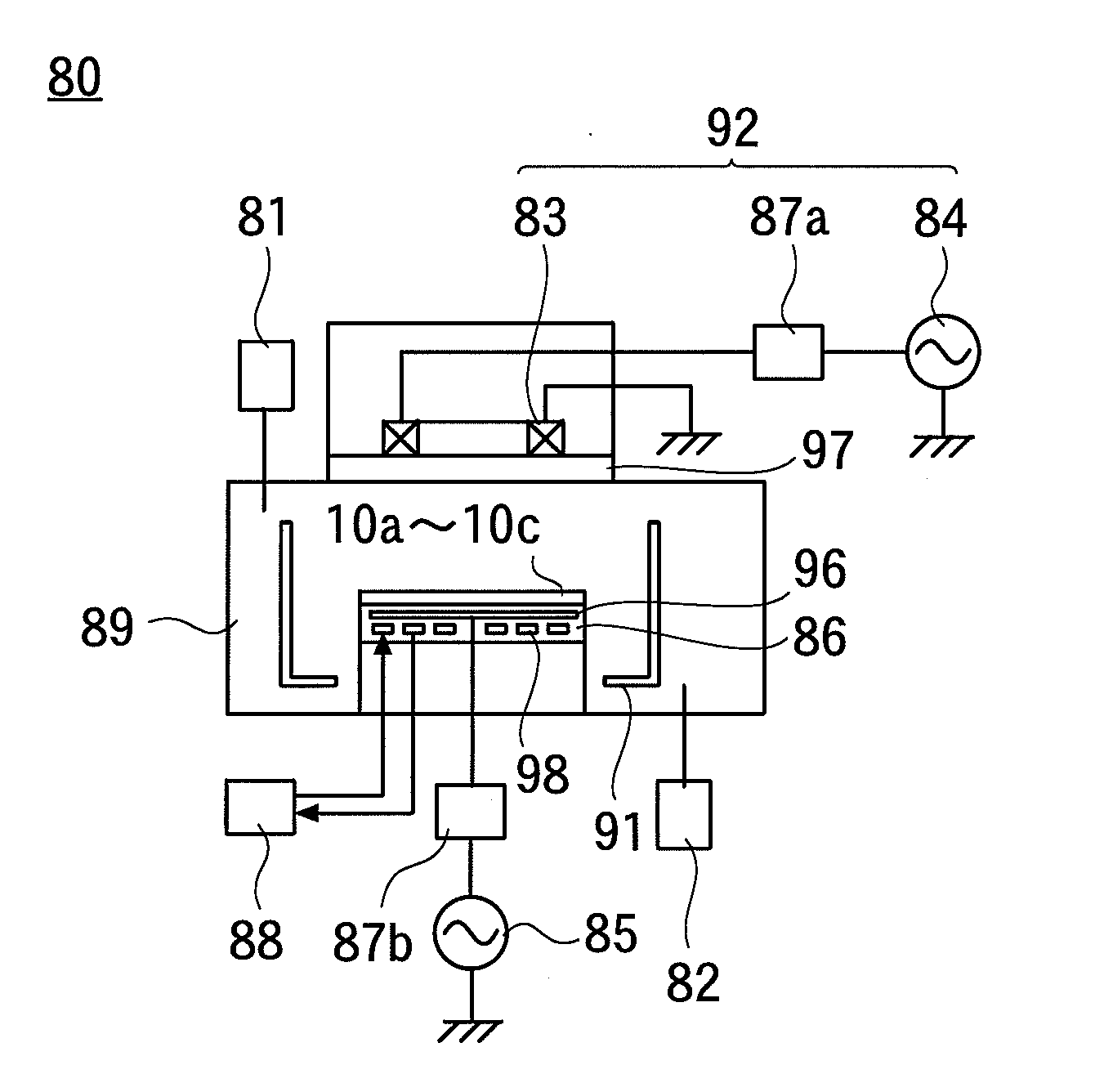
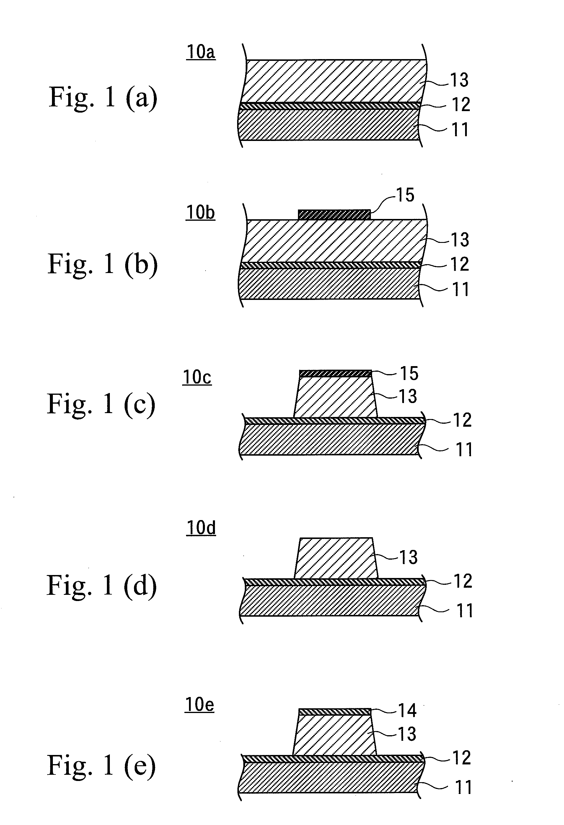
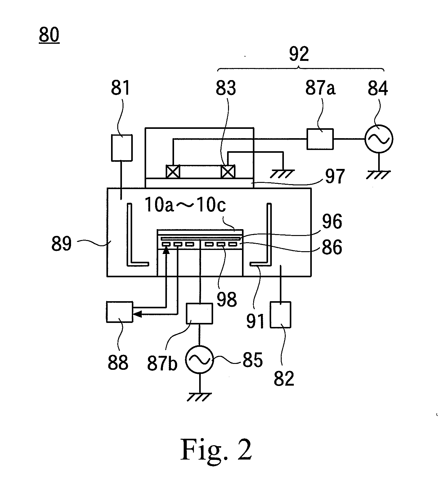
[0067]A PZT film made of PZT was formed on a substrate by the sputtering method and so forth, and then, an object to be processed, in which a Ni mask made of Ni was disposed on the PZT film with the PZT film partly exposed, was carried into the vacuum chamber of the etching apparatus. A temperature control unit is activated, so that the temperature of the object to be processed was controlled so as to be kept at 20° C.

[0068]While evacuating the inside of the vacuum chamber, O2 gas, at a flow rate of 8.4×10⁻³Pa·m3 / sec(5 sccm), and CF4 gas, at a flow rate of 7.6×10⁻²Pa·m3 / sec (45 sccm), were supplied into the inside of the vacuum chamber, as an etching gas, and then the pressure inside the vacuum chamber was set at 0.5 Pa. Here, the flow rate ratio of CF4 gas with respect to the sum of the flow rates of O2 gas and CF4 gas (hereinafter, called CF4 ratio) is 0.9.

[0069]The etching gas was turned into plasma by applying AC power of 600 W to the RF antenna 83 from an AC source...

embodiment 2

[0073]A PZT film made of PZT was formed on a substrate by the sputtering method and so forth; and an object to be processed, in which a Ni mask made of Ni was disposed on the PZT film with the PZT film partly exposed, was photographed by a scanning electron microscope (SEM).

[0074]This object to be processed was carried into the vacuum chamber of the etching apparatus; a mixture gas of O2 gas and CF4 gas, as an etching gas, was supplied into the vacuum chamber; and then, the etching gas was turned into plasma to perform etching.

[0075]Then, after completion of the etching, the object to be processed was taken out of the vacuum chamber and was photographed by the SEM.

[0076]The etched side face was formed with a taper angle of 70°, and no etching products adhered to the side wall.


PUM


Abstract

A method for manufacturing a piezoelectric element, in which a ferroelectric film is processed in an appropriate shape by plasma etching, is provided. A metal mask made of a metal thin film which is hard to be etched by oxygen gas is placed on an object to be processed formed by laminating a lower electrode layer and a ferroelectric film on a substrate in this order. An etching gas containing a mixture gas of the oxygen gas and a reactive gas including fluorine in a chemical structure is turned into plasma and is brought into contact with the metal mask and the object to be processed. An AC voltage is applied to an electrode disposed beneath the object to be processed so that ions in the plasma are caused to enter the object to be processed to perform anisotropic etching on the ferroelectric film.

Description

[0001]This application is a continuation of International Application No. PCT / JP2010 / 062756 filed on Jul. 29, 2010, which claims priority to Japanese Patent Application No. 2009-183047, filed on Aug. 6, 2009. The entire disclosures of the prior applications are herein incorporated by reference in their entireties.BACKGROUND OF INVENTION[0002]The present invention generally relates to a method for manufacturing a piezoelectric element.BACKGROUND ART[0003]In recent years, MEMS (Micro Electro Mechanical Systems) technology has been increasingly developing, and the application range of piezoelectric elements has expanded from industrial instruments to small electronic devices (such as, a driving source for ink discharge used in inkjet recording heads, buzzers, acceleration sensors, hand-shake correction mechanism for digital cameras and so on).[0004]Oxide ferroelectrics, such as lead zirconate titanate (Pb (Zr, Ti) O3, PZT), which have superior piezoelectric property, have been actively...

Claims


Application Information

Patent Timeline
IPC IPC(8): H01L41/22H01L41/332H01L41/39
CPCH01L41/332H10N30/082H02N2/00H10N30/20H10N30/853H10N30/01
Inventor UEDA, MASAHISAYOSHIDA, YOSHIAKIKOKAZE, YUTAKA
Owner ULVAC INC
Why Eureka
Try Eureka