TSV for 3D packaging of semiconductor device and fabrication method thereof
a semiconductor device and 3d packaging technology, applied in semiconductor devices, semiconductor/solid-state device details, electrical apparatus, etc., can solve the problems of limiting the connection fine pitch and high-density electrodes, increasing production costs, and unable to use parts requiring ultrahigh-speed signal processing. achieve the effect of high submicrons, easy alignment of chips, and improved production process efficiency
- Summary
- Abstract
- Description
- Claims
- Application Information
AI Technical Summary
Benefits of technology
Problems solved by technology
Method used
Image

Examples
Embodiment Construction
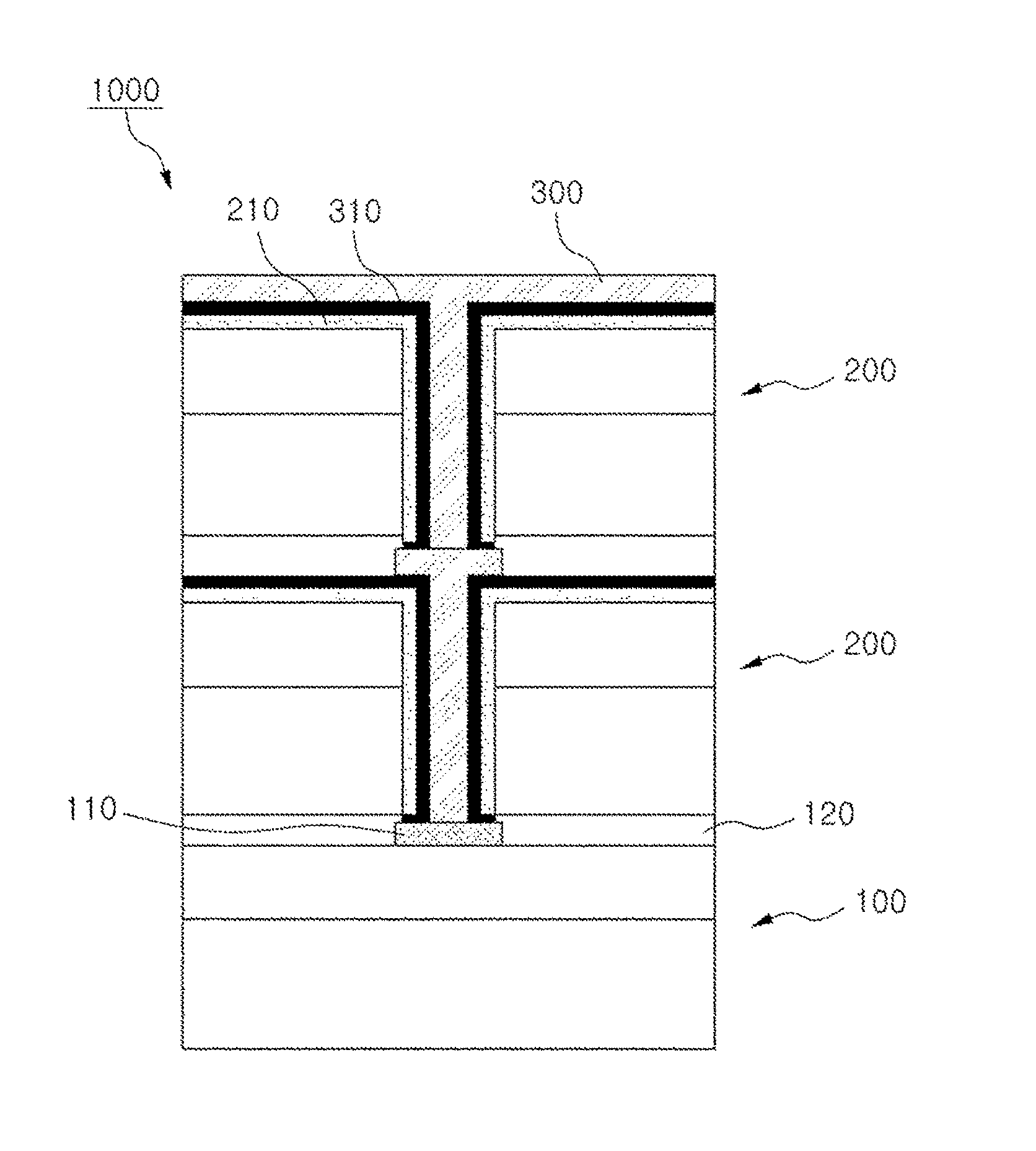
[0036]In general, the through silicon via (TSV), which is a package scheme of forming an electrode by punching a silicon wafer, has been in the limelight as a 3D packaging technology that can remarkably reduce power consumption while preventing high-frequency signal loss and seldom causes a signal delay in order to meet compactness, high speed, and low power performance objectives.
[0037]The through silicon via (TSV) is manufactured by a technology of filling via holes formed on separate silicon wafers (or chips) and then stacking the plurality of wafers (or chips) with the via holes filled.
[0038]Since the wafers with the filled via holes should be provided with bump layers for electrically connecting the wafers with each other, the manufacturing process is difficult and therefore the productivity is degraded.
[0039]Generally, when a via hole is filled by Cu electroplating, the bump layer includes a first bump layer using Cu on the top portion of the Cu layer, and a second bump layer ...
PUM
 Abstract
Description
Claims
Application Information
 - R&D
- Intellectual Property
- Life Sciences
- Materials
- Tech Scout
- Unparalleled Data Quality
- Higher Quality Content
- 60% Fewer Hallucinations
Browse by: Latest US Patents, China's latest patents, Technical Efficacy Thesaurus, Application Domain, Technology Topic, Popular Technical Reports.
© 2025 PatSnap. All rights reserved.Legal|Privacy policy|Modern Slavery Act Transparency Statement|Sitemap|About US| Contact US: help@patsnap.com