Memory Device Having Memory Cells with Enhanced Low Voltage Write Capability

a memory device and write capability technology, applied in the field of semiconductor memory devices, can solve the problems of adversely affecting the performance of the memory device, and unable to prevent local mismatch between the memory, etc., and achieve the effect of accurate low voltage write performan

Active Publication Date: 2012-06-21
AVAGO TECH INT SALES PTE LTD
View PDF8 Cites 21 Cited by
  • Summary
  • Abstract
  • Description
  • Claims
  • Application Information

AI Technical Summary

Benefits of technology

[0009]Illustrative embodiments of the present invention overcome the drawbacks of the conventional approaches described above by providing memory cells in which application of power to respective supply nodes of two cross-coupled inverters of a given memory cell is separately controlled in a manner that ensures accurate low voltage write performance without the need for negative bootstrapping or charge pumps.

Problems solved by technology

As transistor dimensions continue to shrink, it is becoming increasingly difficult to prevent local mismatch between the memory cell transistors of the memory device.
This can adversely impact memory device performance, such as the ability to consistently write data to the memory cells at low voltages.
If in a given memory cell, worst case local variations cause the threshold voltage in the NMOS pass gate transistors to increase and the threshold voltage in the PMOS pull-up transistors to decrease, then the NMOS pass gate transistor coupled to the bitline may not be able to drive the corresponding inverter input below its trip point, and the memory cell will not be written with the data.
This reduced overdrive of the NMOS pass-gate transistor reduces its drive current below the required source current of the PMOS pull-up transistor, leading to the above-noted write failures under worst case local variations.
However, the negative bootstrapping approach has a number of significant drawbacks.
For example, in this approach the bitline negative voltage must be accurately adjusted above the local threshold voltage variation of the NMOS pass gate to ensure smooth write operations, which is very difficult to do in practice, particularly given the presence of variable bitline capacitances across the wide range of rows in a typical embedded memory array.
This could cause the memory cells in unaccessed rows to turn on at very low voltage, potentially leading to inadvertent overwriting of the data stored in those memory cells.
However, this approach requires accurate charge pump circuitry as well as variable pumping capacitance over the wide range of rows of the memory array, and is therefore increasingly difficult to implement as device dimensions shrink.

Method used


Image

  • Memory Device Having Memory Cells with Enhanced Low Voltage Write Capability
  • Memory Device Having Memory Cells with Enhanced Low Voltage Write Capability
  • Memory Device Having Memory Cells with Enhanced Low Voltage Write Capability

Examples


Embodiment Construction

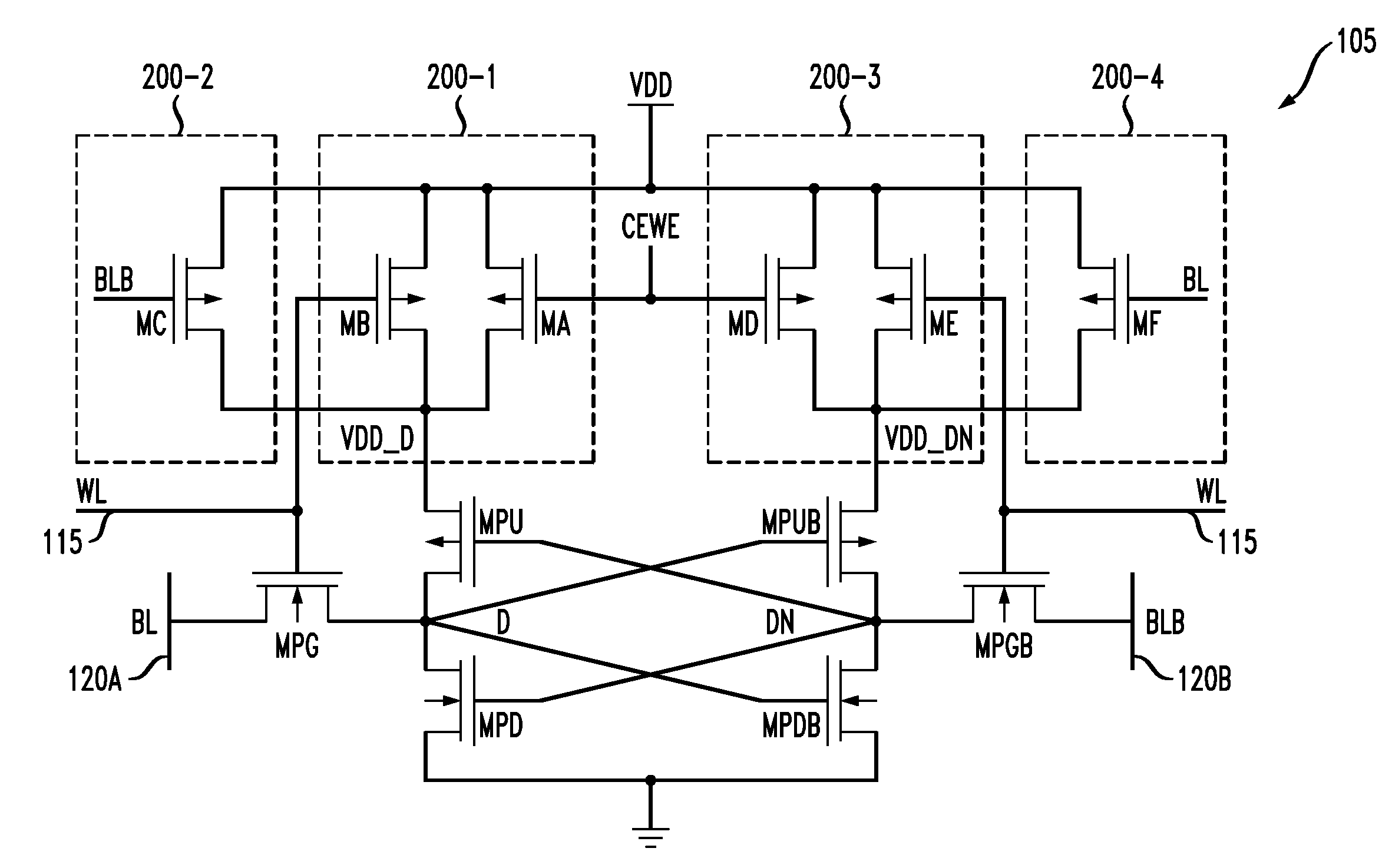
[0024]The invention will be illustrated herein in conjunction with exemplary semiconductor memory devices and associated memory cells as well as other related circuitry. It should be understood, however, that the invention is more generally applicable to any semiconductor memory device in which improved low voltage write performance is desired, and may be implemented using circuitry other than that specifically shown and described in conjunction with the illustrative embodiments.

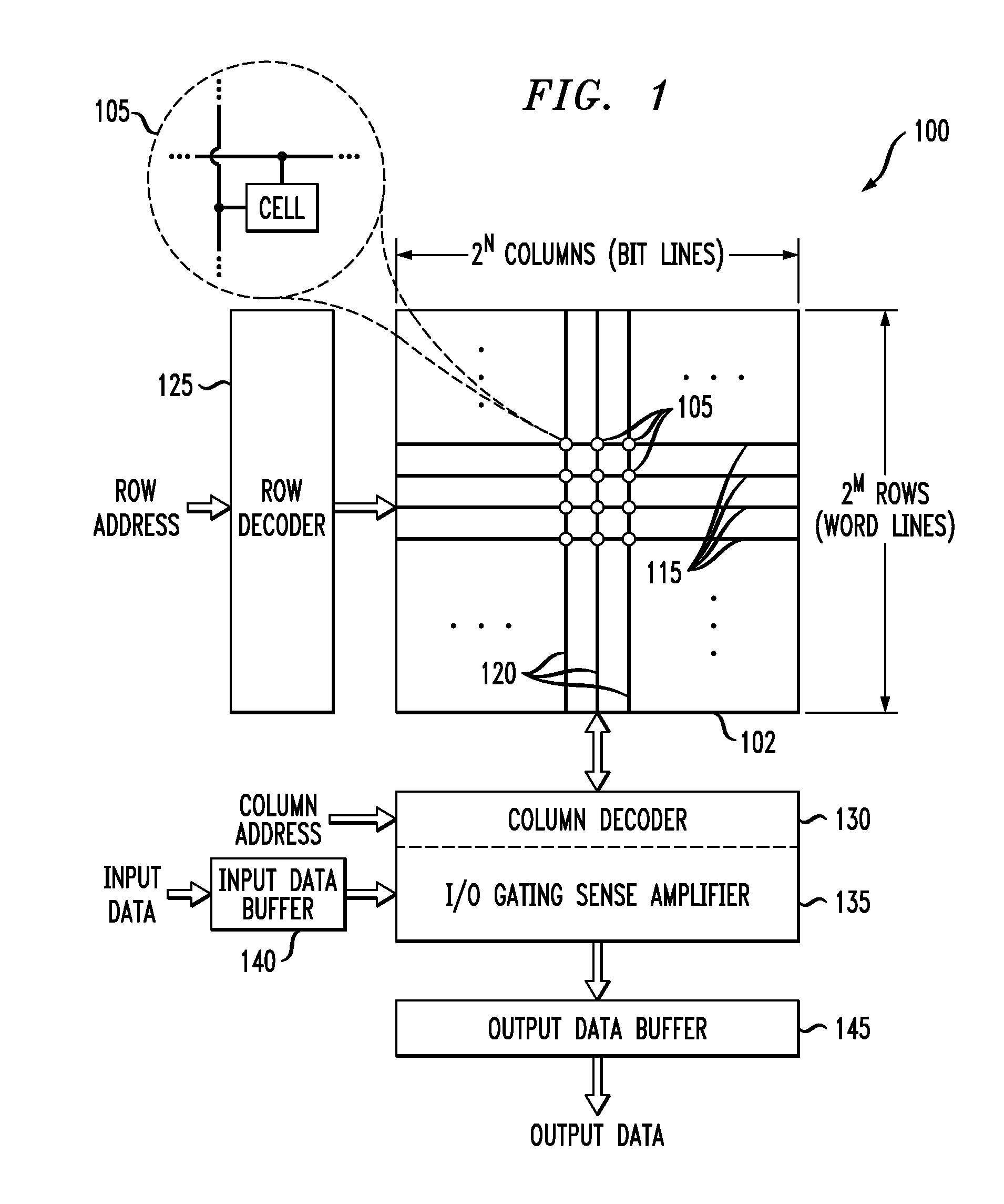
[0025]FIG. 1 shows a simplified diagram of a memory device 100 in accordance with an illustrative embodiment of the invention. The memory device 100 comprises a memory array 102. The memory array 102 comprises a plurality of memory cells 105 each configured to store data. For example, the memory cells may each be configured to store a single bit of data, and such memory cells are also referred to herein as bit-cells. Each cell 105 is coupled to a corresponding row or wordline 115 and column or bitline 120. T...


PUM


Abstract

A memory device includes a memory array comprising a plurality of memory cells. At least a given one of the memory cells comprises a pair of cross-coupled inverters and associated write assist circuitry. The write assist circuitry comprises first switching circuitry coupled between a supply node of a device of the first inverter and a supply node of the memory cell, and second switching circuitry coupled between a supply node of a device of the second inverter and the supply node of the memory cell. The first and second switching circuitry are separately controlled such that during a write operation of the memory cell the supply node of one of the devices is connected to the supply node of the memory cell while the supply node of the other device is not connected to the supply node of the memory cell but is instead permitted to float.

Description

FIELD OF THE INVENTION[0001]The present invention relates generally to semiconductor memory devices, and more particularly to techniques for configuring such devices to permit write operations to occur at reduced voltage levels.BACKGROUND OF THE INVENTION[0002]A semiconductor memory device typically includes an array of memory cells arranged in rows and columns, with each memory cell configured to store one or more bits of data. The memory cells within a given row of the array are coupled to a common wordline, while the memory cells within a given column of the array are coupled to a common bitline. Thus, the array includes a memory cell at each point where a wordline intersects with a bitline.[0003]In a semiconductor memory device of the type described above, data may be written to or read from the memory cells of the array using a memory cycle that is divided into a precharge phase and an active phase, with the precharge phase being used to precharge the bitlines to a precharge vo...

Claims


Application Information

Patent Timeline
Patent Type & Authority Applications(United States)
IPC IPC(8): G11C11/419
CPCG11C11/419G11C11/412
Inventor RACHAMADUGU, VINODRAO, SETTI SHANMUKHESWARAGOWDA, SATISHA NANJUNDE
Owner AVAGO TECH INT SALES PTE LTD
Why Eureka
Try Eureka