Computer simulation of photolithographic processing

a photolithographic processing and computer simulation technology, applied in the field of computer simulation of photolithographic processing, can solve the problems of affecting the effect of mask optimization, and increasing the difficulty of adjusting the mask, so as to achieve sufficient fast simulation, increase the ease of mask optimization, and speed up the computation time

Inactive Publication Date: 2012-06-21
OLAMBDA
View PDF0 Cites 5 Cited by
  • Summary
  • Abstract
  • Description
  • Claims
  • Application Information

AI Technical Summary

Benefits of technology

[0007]Notably, a typical thickness of the resist film 114 can be in the range of 100 nm-1000 nm and a desired height of the L-shaped feature on the etched wafer structure 130 can be hundreds of nanometers, while the desired line width of the L-shaped feature may be well under 100 nm (for example, 45 nm, 32 nm, and even 22 nm or below). In view of these very high aspect ratios, it becomes important for a simulation system to properly accommodate for the truly three-dimensional nature of the optical and chemical interactions that are taking place during the photolithographic process in order to be accurate. At same time, in view of the above-described iterative nature of the mask optimization process, it is desirable for the simulation results to be provided in a practicably short period of time, with increased ease of mask optimization being associated with faster computation times. Especially in view of the staggering amount of data associated with today's ever-shrinking and increasingly complex circuit patterns, there is a tension between providing sufficiently accurate simulations and providing sufficiently fast simulations.

Problems solved by technology

In particular, the optical projection of circuit patterns onto semiconductor wafers, during a process known as photolithography, becomes increasingly complicated to predict as pattern sizes shrink well below the wavelength of the light that is used to project the pattern.
Unfortunately, the required “corrections” or pre-compensations are themselves difficult to refine and, although there are some basic pre-compensation rules that a human designer can start with, the pre-compensation process is usually iterative (i.e., trial and error) and pattern-specific to the particular desired circuit pattern.
While certain prior art approaches such as those based on differential-equation-solving techniques, finite difference techniques, or finite element techniques can provide accurate results, even to the extent of representing a kind of gold standard in their accuracy, they are generally quite slow.
However, many prior art closed-form techniques are believed to suffer from one or more shortcomings that are addressed by one or more of the preferred embodiments described hereinbelow.
For example, many prior art closed-form techniques either ignore the third dimension altogether or are based on mathematical models do not adequately accommodate for the real-world, high aspect ratio, three-dimensional character of the interactions taking place.
By way of further example, many of the above prior art techniques are unable to efficiently accommodate process variations in the photolithographic systems being modeled, and thus for each combination of values for physical variations in the photolithographic process (such as bake temperature, resist development time, etchant pH, stepper defocus parameter, etc.), such techniques require the entire (or almost entire) simulation process to be repeated essentially from the beginning.

Method used


Image

  • Computer simulation of photolithographic processing
  • Computer simulation of photolithographic processing
  • Computer simulation of photolithographic processing

Examples


Embodiment Construction

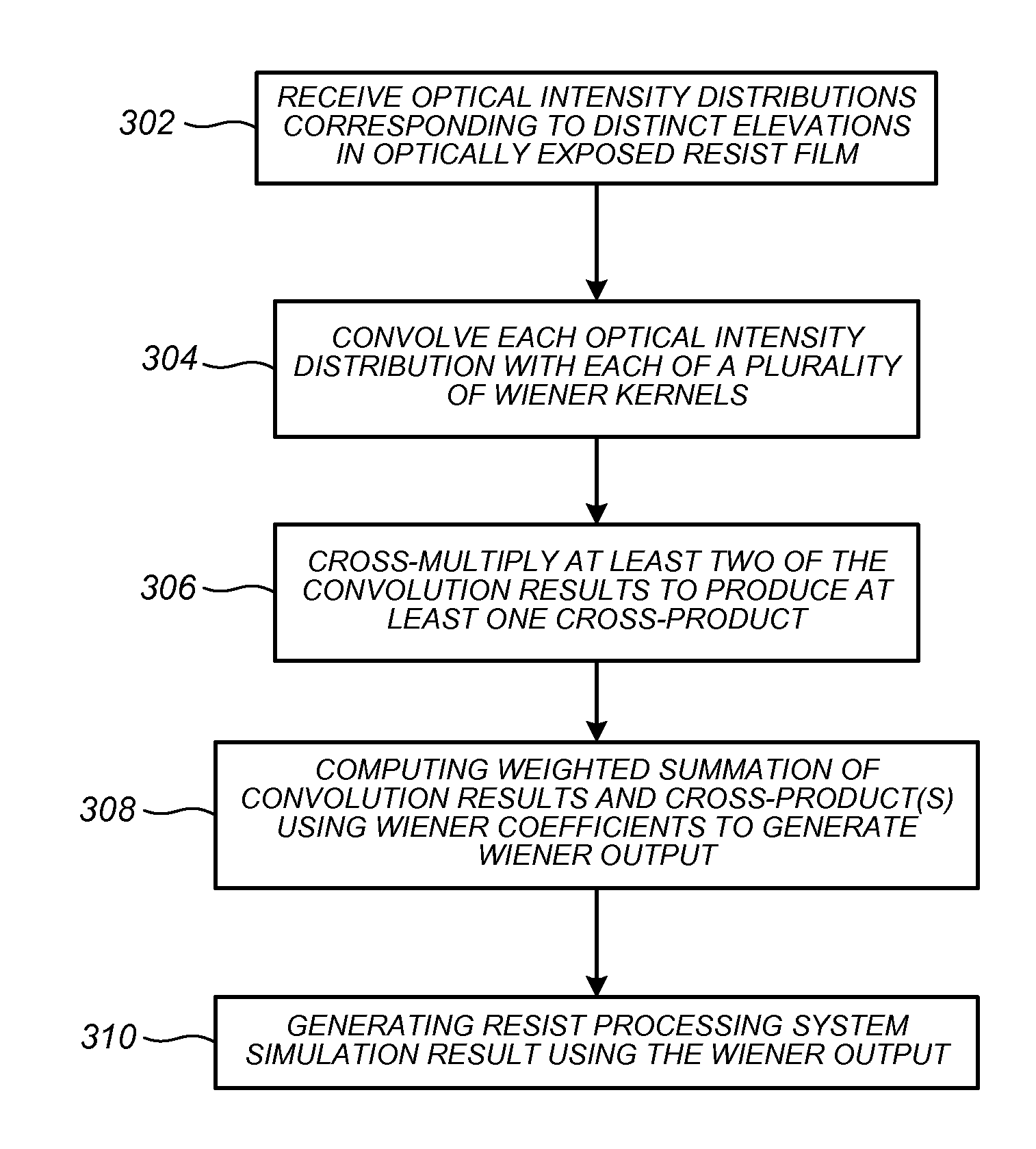
[0043]FIG. 3 illustrates simulating a resist processing system according to a preferred embodiment, which is described herein in conjunction with FIG. 4 that illustrates a resist processing system simulation model according to a preferred embodiment. Referring first to FIG. 4, the resist processing system simulation model comprises a first portion 402 which comprises operations falling into the Wiener class and which is referenced hereinafter as Wiener operator 402. The model further comprises a second portion 422 which comprises at least one operation (here, a thresholding operation) that does not fall into the Wiener class and which is referenced hereinafter as non-Wiener operator 422. A discussion of operations inside and outside the Wiener class can be found in Schetzen, M., “Nonlinear System Modeling Based on the Wiener Theory,” Proceedings of the IEEE, Vol. 69, No. 12 (1981), which is incorporated by reference herein.

[0044]Wiener operator 402 comprises a convolution operator 4...


PUM


Abstract

Methods, systems, and related computer program products for photolithographic process simulation are disclosed. In one preferred embodiment, a resist processing system is simulated according to a Wiener nonlinear model thereof in which a plurality of precomputed optical intensity distributions corresponding to a respective plurality of distinct elevations in an optically exposed resist film are received, each optical intensity distribution is convolved with each of a plurality of predetermined Wiener kernels to generate a plurality of convolution results, and at least two of the convolution results are multiplied to produce at least one cross-product. A weighted summation of the plurality of convolution results and the at least one cross-product is computed using a respective plurality of predetermined Wiener coefficients to generate a Wiener output, and a resist processing system simulation result is generated based at least in part on the Wiener output.

Description

CROSS-REFERENCE TO RELATED APPLICATIONS[0001]This patent application claims the benefit of U.S. Provisional Ser. No. 60 / 948,467 filed Jul. 8, 2007, which is incorporated by reference herein. This patent application is a continuation-in-part of U.S. Ser. No. 11 / 708,444 filed Feb. 20, 2007, which is a continuation-in-part of U.S. Ser. No. 11 / 331,223, filed Jan. 11, 2006, now abandoned, each of which is incorporated by reference herein.FIELD[0002]This patent specification relates to computer simulation of photolithographic processes as may be employed, for example, in sub-wavelength integrated circuit fabrication environments.BACKGROUND AND SUMMARY[0003]Computer simulation has become an indispensable tool in a wide variety of technical endeavors ranging from the design of aircraft, automobiles, and communications networks to the analysis of biological systems, socioeconomic trends, and plate tectonics. In the field of integrated circuit fabrication, computer simulation has become incre...

Claims


Application Information

Patent Timeline
Patent Type & Authority Applications(United States)
IPC IPC(8): G06F17/10G06F7/60
CPCG03F1/36G06F17/5018G03F7/705G06F30/23
Inventor WEI, HAIQING
Owner OLAMBDA
Why Eureka
Try Eureka