Semiconductor device

a semiconductor device and semiconductor technology, applied in the direction of solid-state devices, transistors, instruments, etc., can solve the problems of difficult to sufficiently reduce power consumption, short data holding period, and high cost per storage capacity, so as to improve the degree of integration of a semiconductor device, increase storage capacity per unit area, and reduce the area occupied by memory cells

Active Publication Date: 2012-06-28
SEMICON ENERGY LAB CO LTD
View PDF7 Cites 42 Cited by
  • Summary
  • Abstract
  • Description
  • Claims
  • Application Information

AI Technical Summary

Benefits of technology

[0028]Further, in the semiconductor device according to one embodiment of the present invention, a gate electrode of a transistor including a semiconductor material other than an oxide semiconductor serves as one of a source electrode and a drain electrode of a transistor including an oxide semiconductor, whereby one of the source elect...

Problems solved by technology

Moreover, a transistor included in a memory element has leakage current (off-state current) between a source and a drain in an off state or the like and electric charge flows into or out of the transistor even if the transistor is not selected, which makes a data holding period short.
For that reason, a writing operation (refresh operation) is necessary at predetermined intervals, and it is difficult to sufficiently reduce power consumption.
Furthermore, since stored data is lost when power supply stops, another memory device utilizing a magnetic material or an optical material is needed in order to hold the data for a long time.
However, cost per storage capacity is higher because a circuit such as a flip-flop is used.
Moreover, as in a DRAM, stored data in an SRAM is lost when power supply stops.
However, in a flash...

Method used


Image

  • Semiconductor device
  • Semiconductor device
  • Semiconductor device

Examples


embodiment 1

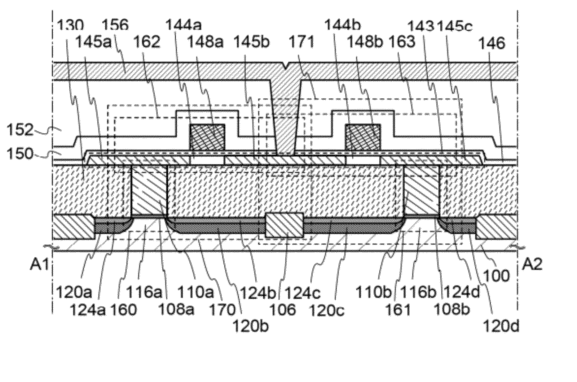
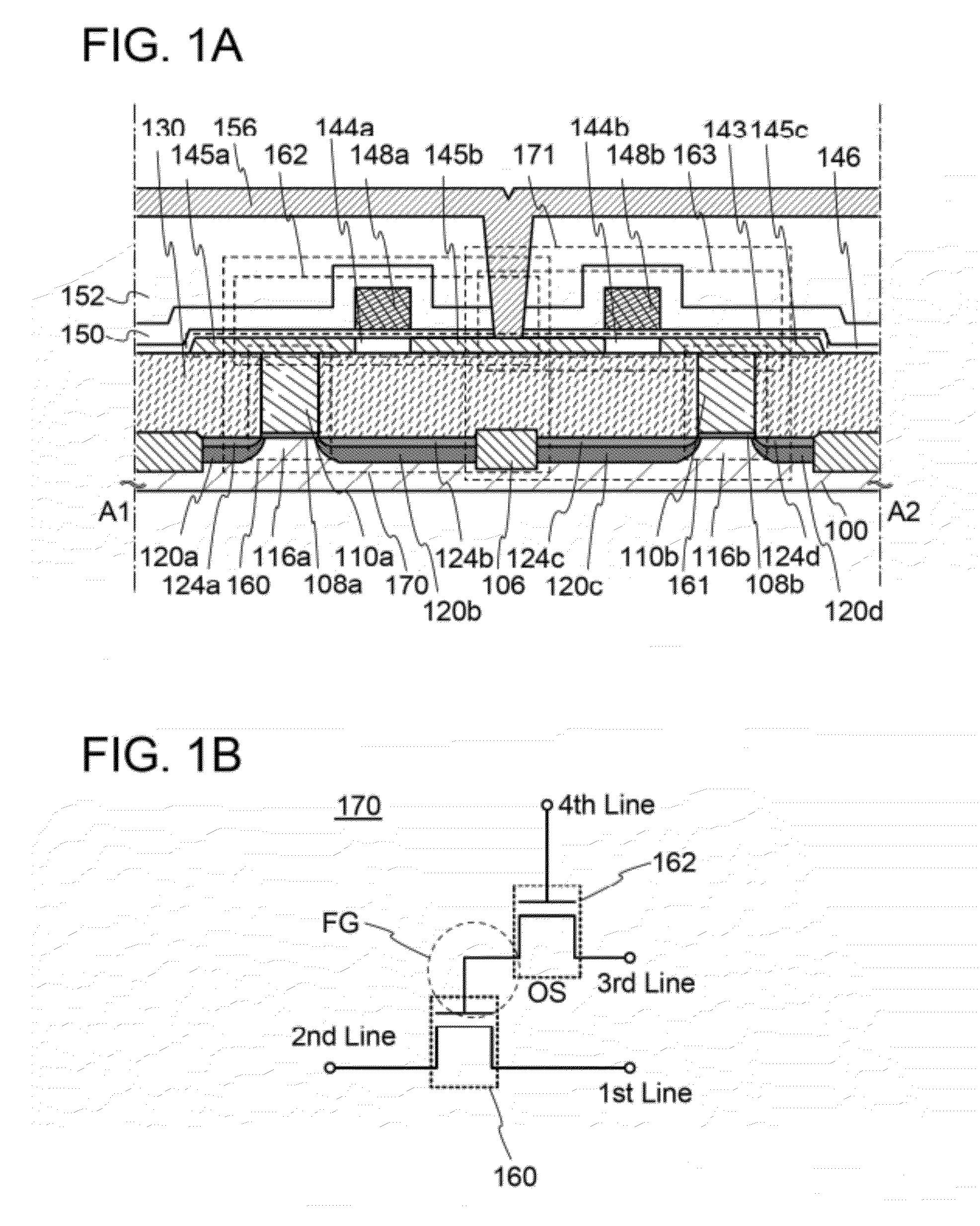
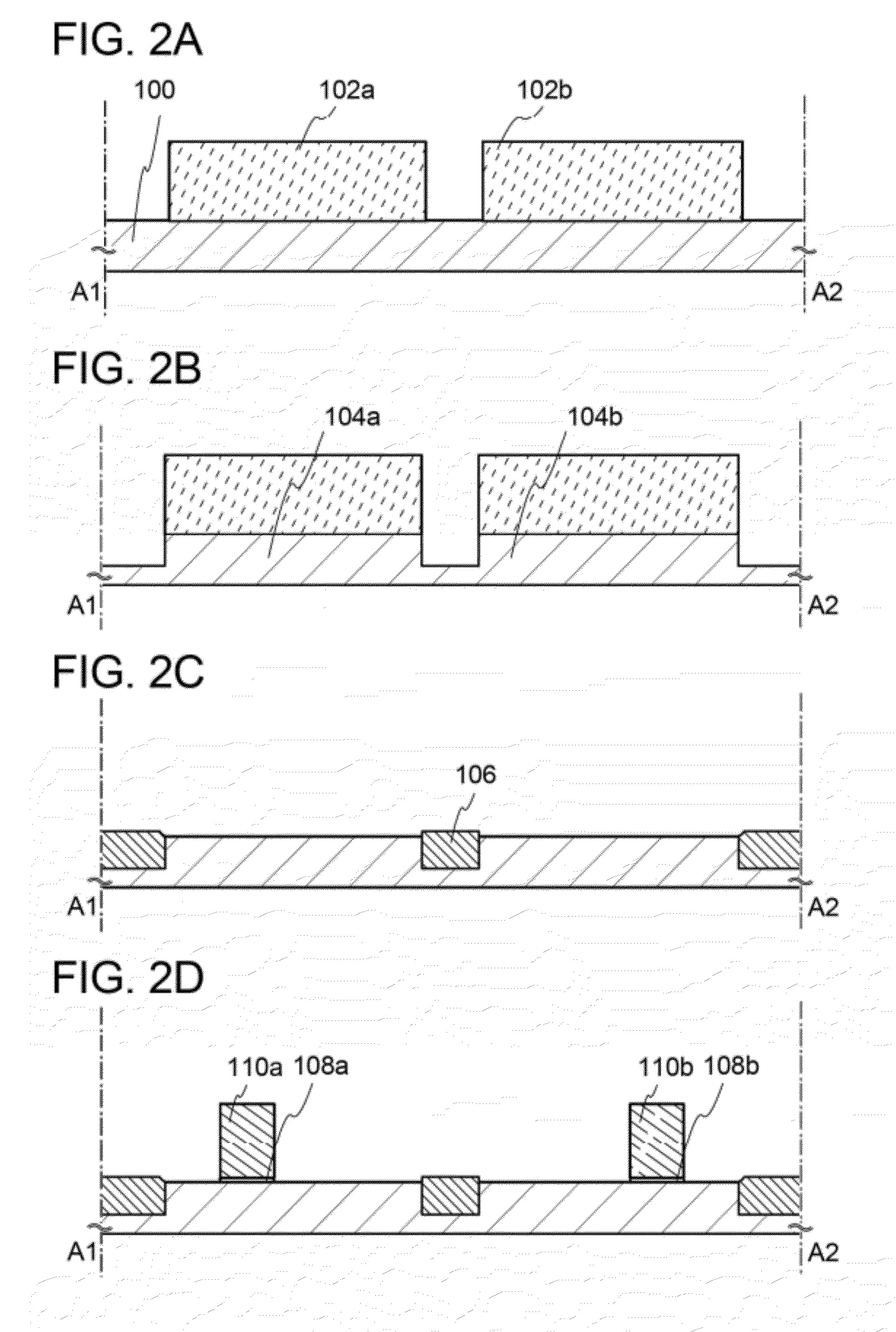
[0046]In this embodiment, a structure and a manufacturing method of semiconductor devices according to one embodiment of the present invention will be described with reference to FIGS. 1A and 1B, FIGS. 2A to 2D, FIGS. 3A to 3D, FIGS. 4A to 4C, and FIGS. 5A to 5C.

[0047]FIGS. 1A and 1B illustrate an example of a structure of the semiconductor device. FIG. 1A is a cross-sectional view of the semiconductor device, and FIG. 1B is a circuit diagram of the semiconductor device. The semiconductor device in FIGS. 1A and 1B can be used as a memory device. Note that the semiconductor device illustrated in FIGS. 1A and 1B is just an example of a semiconductor device having predetermined functions and does not represent all semiconductor devices according to one embodiment of the present invention. The semiconductor device according to one embodiment of the present invention can have another function by changing connection of an electrode or the like as appropriate.

[0048]The semiconductor device...

embodiment 2

[0148]In this embodiment, a semiconductor device partly different from the semiconductor device shown in the above embodiment is described with reference to FIGS. 6A and 6B and FIGS. 7A to 7D. Note that in this embodiment, only different portions from the above embodiment will be described.

[0149]FIG. 6A is a cross-sectional view of the semiconductor device, and FIG. 6B is a circuit diagram of the semiconductor device. The semiconductor device in FIGS. 6A and 6B can also be used as a memory device.

[0150]The semiconductor device illustrated in FIG. 6A includes, in a lower portion, the transistors 160 and 161, and in an upper portion, the transistors 162 and 163, a capacitor 164, and a capacitor 165. In addition, the transistors 160 and 162 and the capacitor 164 can form a memory cell 172, and the transistors 161 and 163 and the capacitor 165 can form a memory cell 173.

[0151]The capacitor 164 includes the gate electrode 110a, the oxide semiconductor layer 143, the gate insulating layer...

embodiment 3

[0171]In this embodiment, a semiconductor device partly different from the semiconductor device shown in the above embodiment is described with reference to FIG. 8 and FIGS. 9A to 9C. Note that in this embodiment, only different portions from the above embodiment will be described.

[0172]The semiconductor device illustrated in FIG. 8 includes, in a lower portion, the transistors 160 and 161, and in an upper portion, a transistor 166, a transistor 167, a capacitor 168, and a capacitor 169. In addition, the transistors 160 and 166 and the capacitor 168 can form a memory cell 174, and the transistors 161 and 167 and the capacitor 169 can form a memory cell 175. Note that the structures of the transistors 160 and 161 in the lower portion are similar to those of the transistors 160 and 161 illustrated in FIG. 6A and thus is not described in detail.

[0173]The capacitor 168 includes the gate electrode 110a, the oxide semiconductor layer 143, the gate insulating layer 146, and the electrode 1...


PUM

PropertyMeasurementUnit
Electrical resistanceaaaaaaaaaa
Electrical conductoraaaaaaaaaa
Semiconductor propertiesaaaaaaaaaa

Abstract

The degree of integration of a semiconductor device is enhanced and the storage capacity per unit area is increased. The semiconductor device includes a first transistor provided in a semiconductor substrate and a second transistor provided over the first transistor. In addition, an upper portion of a semiconductor layer of the second transistor is in contact with a wiring, and a lower portion thereof is in contact with a gate electrode of the first transistor. With such a structure, the wiring and the gate electrode of the first transistor can serve as a source electrode and a drain electrode of the second transistor, respectively. Accordingly, the area occupied by the semiconductor device can be reduced.

Description

BACKGROUND OF THE INVENTION[0001]1. Field of the Invention[0002]The disclosed invention relates to a semiconductor device using a semiconductor element and a method for driving the semiconductor device.[0003]2. Description of the Related Art[0004]Memory devices using semiconductor elements are broadly classified into two categories: a volatile memory device that loses stored data when power supply stops, and a nonvolatile memory device that holds stored data even when power is not supplied.[0005]A typical example of a volatile memory device is a dynamic random access memory (DRAM). A DRAM stores data in such a manner that a transistor included in a memory element is selected and electric charge is stored in a capacitor.[0006]When data is read from a DRAM, electric charge in a capacitor is lost according to the above-described principle; thus, another writing operation is necessary every time data is read out. Moreover, a transistor included in a memory element has leakage current (o...

Claims


Application Information

Patent Timeline
IPC IPC(8): H01L29/94H01L27/088
CPCH01L27/1156H01L27/1225G11C13/0004C04B2235/3286C04B35/58C04B2235/3284G11C16/0433H10B41/70H10B99/00H10B12/00H01L27/1207H10B41/20
Inventor YAMAZAKI, SHUNPEI
Owner SEMICON ENERGY LAB CO LTD
Why Eureka
Try Eureka