Lithography system and method of processing substrates in such a lithography system

a lithography system and substrate technology, applied in the field of lithography systems, can solve the problems of reducing the throughput of 10 times, the cost of the floor space in the semiconductor manufacturing environment, etc., and achieve the effect of reducing the cost of lithography system maintenance, and ensuring the quality of lithography

a lithography system and substrate technology, applied in the field of lithography systems, can solve the problems of reducing the throughput of 10 times, the cost of the floor space in the semiconductor manufacturing environment, etc., and achieve the effect of reducing the cost of lithography system maintenance, and ensuring the quality of lithography

US20120175527A1Active Publication Date: 2012-07-12ASML NETHERLANDS BV

Image

  • Lithography system and method of processing substrates in such a lithography system
  • Lithography system and method of processing substrates in such a lithography system
  • Lithography system and method of processing substrates in such a lithography system

Examples


Embodiment Construction

[0033]The following is a description of various embodiments of the invention, given by way of example only and with reference to the drawings.

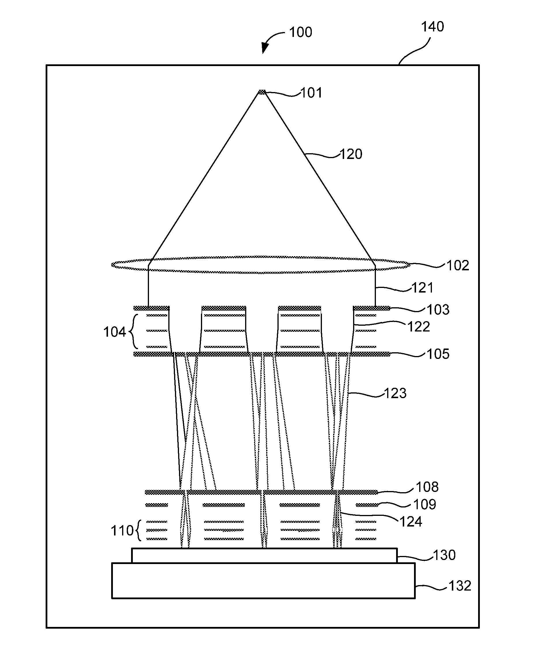
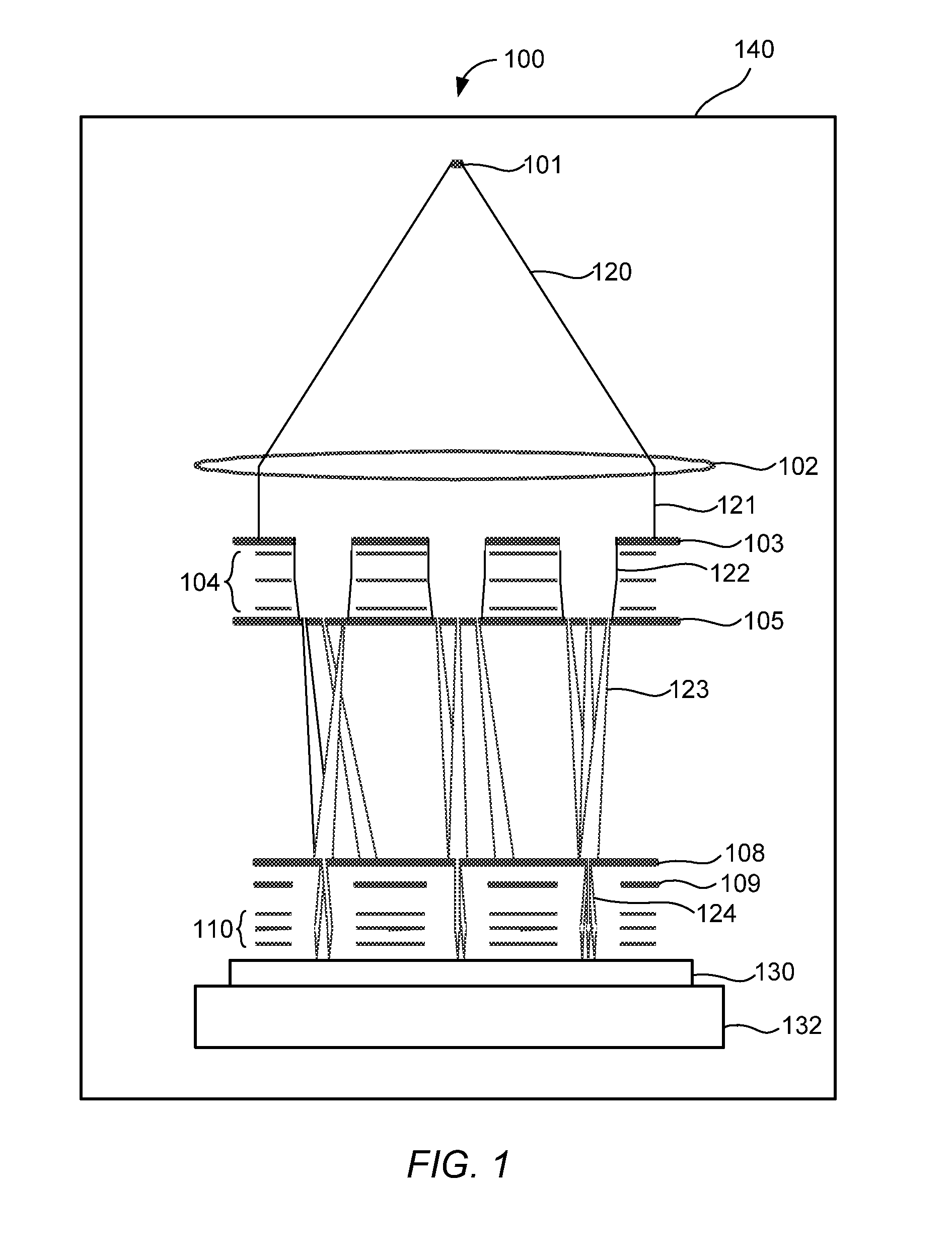
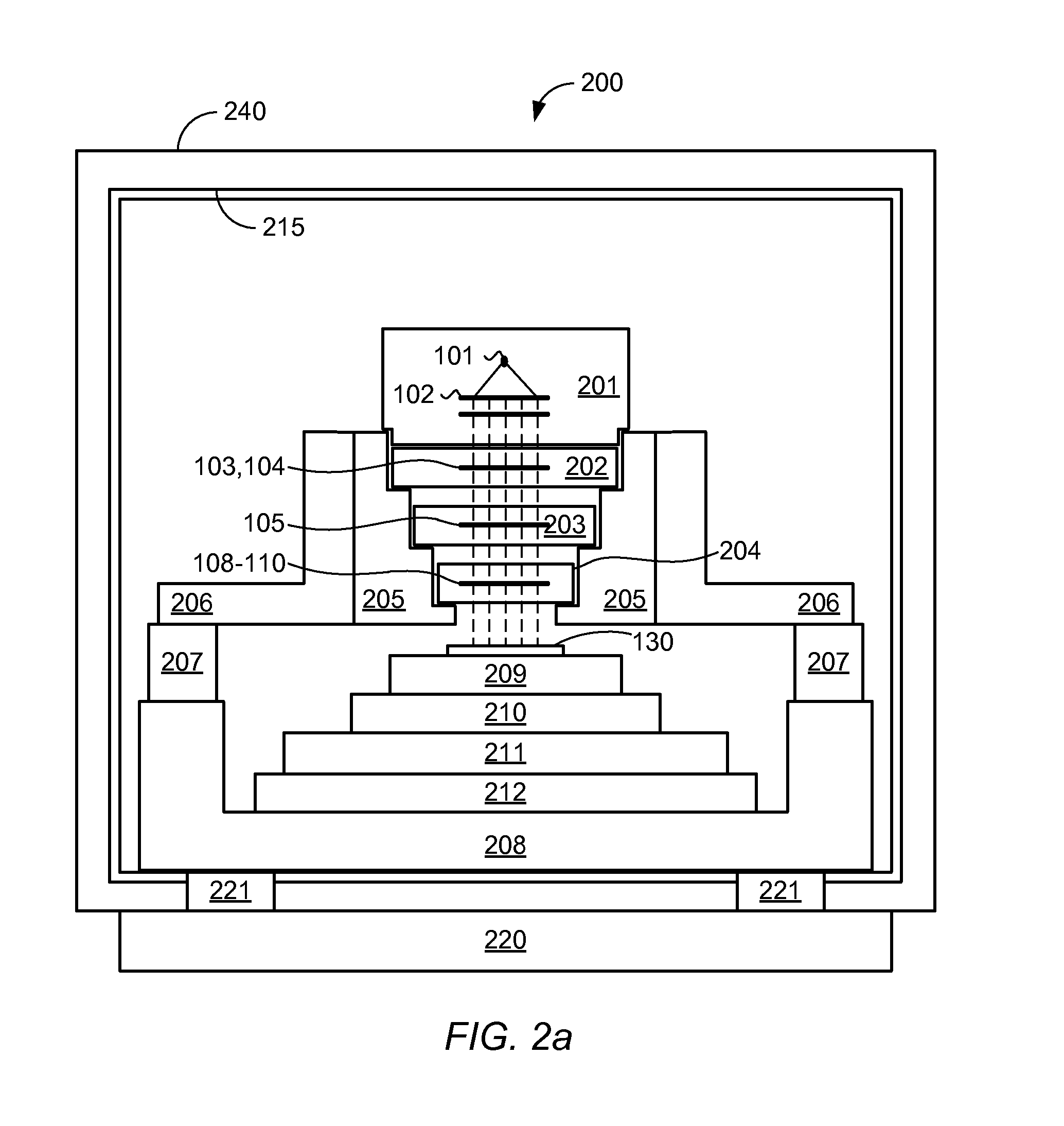
[0034]FIG. 1 shows a simplified schematic drawing of an embodiment of a charged particle lithography apparatus 100. Such lithography systems are described for example in U.S. Pat. Nos. 6,897,458 and 6,958,804 and 7,019,908 and 7,084,414 and 7,129,502, U.S. patent application publication no. 2007 / 0064213, and co-pending U.S. patent application Ser. Nos. 61 / 031,573 and 61 / 031,594 and 61 / 045,243 and 61 / 055,839 and 61 / 058,596 and 61 / 101,682, which are all assigned to the owner of the present invention and are all hereby incorporated by reference in their entirety.

[0035]In the embodiment shown in FIG. 1, the lithography apparatus 100 comprises an electron source 101 for producing an expanding electron beam 120. The expanding electron beam 120 is collimated by collimator lens system 102. The collimated electron beam 121 impinges on an aperture array...


PUM


Abstract

The invention relates to a lithography system comprising a plurality of lithography system units. Each lithography system unit comprises a lithography apparatus arranged in a vacuum chamber for patterning a substrate; a load lock system for transferring substrates into and out of the vacuum chamber; and a door for enabling entry into the vacuum chamber for servicing purposes. The load lock system and the door of each lithography system unit are provided at the same side and face a free area at a side of the lithography system, in particular the service area.

Description

BACKGROUND OF THE INVENTION[0001]1. Field of the Invention[0002]The present invention generally relates to a lithography system comprising a plurality of lithography system units. The invention further relates to a method of handling substrates in such a lithography system.[0003]2. Description of the Related Art[0004]In the semiconductor industry, an ever increasing desire to manufacture smaller structures with high accuracy and reliability puts great demands on wafer processing technology. In particular, it is important to maximize wafer throughput of wafer processing equipment while maintaining the lowest capital costs and operational costs, and without excessive use of floor space. Floor space in a semiconductor manufacturing environment is expensive, as most space needs to meet high standard clean room conditions. Therefore, the floor space that is to be occupied by wafer processing equipment, i.e. the so-called footprint, is preferably as limited as possible. Furthermore, to en...

Claims


Application Information

Patent Timeline
12 Jul 2012
Publication
US20120175527A1
IPC
G21K5/08; G21K5/00
CPC
G03F7/708; G03F7/70808; H01J2237/31774; H01J37/16; H01J37/185; G03F7/70975
Inventors
DE BOER, GUIDO; DE JONG, HENDRIK JAN