
Multi chip module, method for operating the same and dc/dc converter

a multi-chip module and converter technology, applied in the direction of process and machine control, instrumentation, and semiconductor/solid-state device details, etc., can solve the problems of insufficient accuracy, increased cost, and damage to efficiency, and achieve cost-effective and accurate current sensing

Active Publication Date: 2012-07-19
TEXAS INSTR INC
View PDF12 Cites 37 Cited by
  • Summary
  • Abstract
  • Description
  • Claims
  • Application Information

AI Technical Summary

Benefits of technology

[0005]It is a general object of the present invention to provide a multi chip module, a method for operating the same and a DC / DC converter that allows a cost effective and accurate current sensing at the switching node of a half bridge configuration that is a part of the multi chip module and the DC / DC converter, respectively.
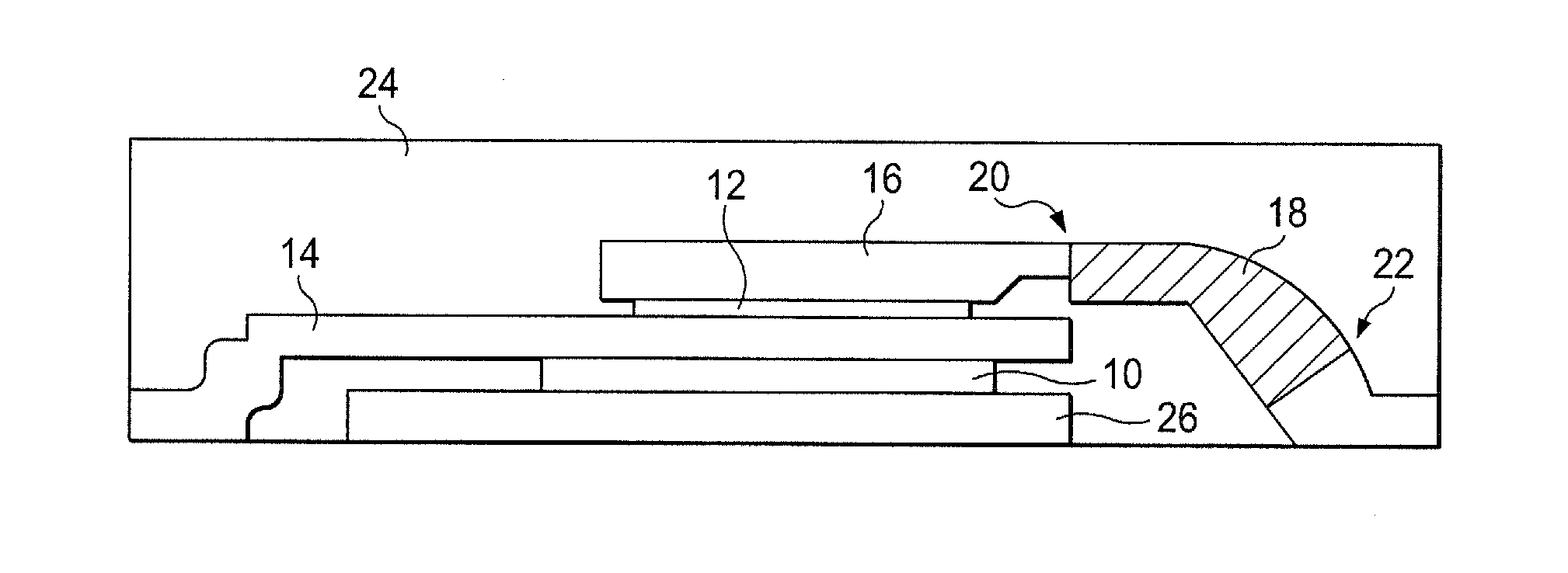
[0009]The multi chip module makes use of the on-resistance of the tap clip of the vertically stacked field effect transistor configuration for determination of the current that is provided to the switching node via said tap clip. According to the invention, the multi chip module does not need an extra shunt resistor. It is a compact and highly integrated solution providing an opportunity for precise DCR current sensing at the switching node. Further, an embedded solution for DCR current sensing is provided. No additional losses occur and, at the same time, the accuracy of the DCR current sensing is improved. No additional board space is required especially if the current sensing circuit is integrated into a controller circuit that is controlling the semiconductor half bridge configuration.
[0014]According to another aspect of the invention, the predetermined distance between the two checkpoints, a thickness and / or a material of the tap clip comprising the at least one checkpoint, may be selected so as to provide a predetermined resistance of the shunt resistor. The tap clips of the stacked semiconductor configuration are a mechanical implementation and, accordingly, it is easily possible to modify i.e., a thickness of the tap, clip in order to modify its on resistance. This allows an easy adjustment of the on-resistance without causing excessive heat-up of the overall implementation.
[0015]The tap clips are made of copper which provides a high electrical and thermal conductance. Instead of staying with the copper clip implementation, according to another aspect of the invention, at least the tap clip comprising the at least one checkpoint may be made of a manganine alloy. Manganine is a commonly used name for an alloy of typically 86% copper, 12% manganese and 2% nickel. Manganine provides the advantage of virtually having a zero temperature coefficient of resistance. Further, it offers long-term stability. The use of manganine simplifies the current sensing circuit since the need of a temperature-dependent compensation is no longer present. According to another advantageous aspect of the invention, the lead frame of the multi chip module is also made of a manganine alloy. This allows performing a more accurate high-side FET or low-side FET current sensing in case this is desired.
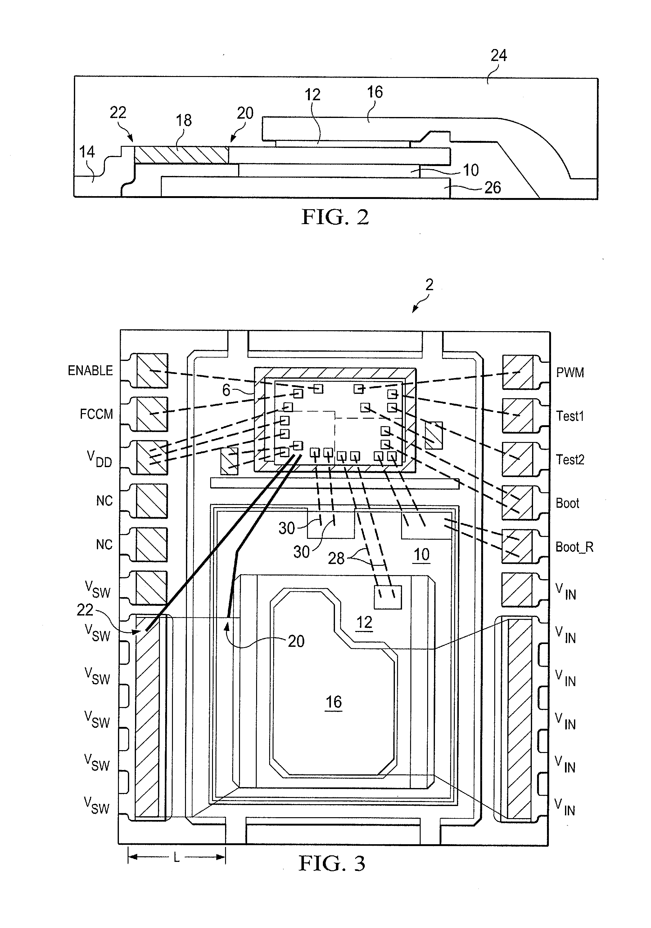
[0016]In another aspect of the invention, the multi chip module has a layout wherein the current sensing circuit and the semiconductor half bridge configuration share a common lead frame and the current sensing circuit is positioned next to or on top of the semiconductor half bridge configuration. In the latter layout, the current sensing circuit is stacked on top of the drain clip of the high-side FET. This layout saves space and increases the power density. Further, the current sensing circuit may be integrated into a controller circuit for driving the semiconductor half bridge configuration.
[0020]The same or similar advantages already mentioned for the multi chip module apply to the DC / DC converter according to the invention. In particular, the DC / DC converter allows a cost effective, reliable and accurate measurement of the current provided to the inductance of the converter.

Problems solved by technology

However, those implementations hurt the efficiency and are usually not as accurate as desired.
Especially in mass production trimming and tolerances, as this means additional cost.
Further, it is expected that in near future, the switching frequencies of the DC / DC converters will increase, which means that the inductance value of the inductor will become smaller, which in turn will result in a significantly lower on-resistance of the inductor.
This will cause severe difficulties in reading out the current in the inductor by making use of the small DCR of its copper windings.
Again, a shunt resistor may be applied for DCR current sensing, which will however cause an additional power loss.
Further, an expensive and precise shunt sense resistor is needed.
This could be achieved by laser trimming the printed copper trace, but again, this would cause additional costs and would increase production complexity.

Method used


Image

  • Multi chip module, method for operating the same and dc/dc converter
  • Multi chip module, method for operating the same and dc/dc converter
  • Multi chip module, method for operating the same and dc/dc converter

Examples


Embodiment Construction

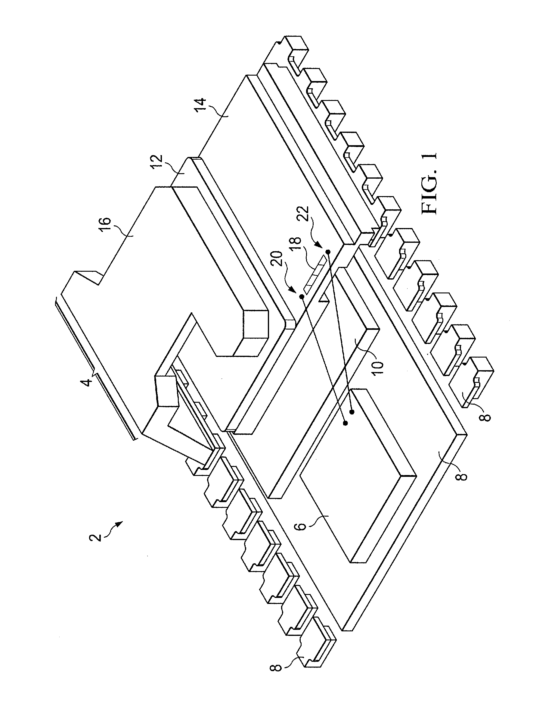
[0029]FIG. 1 is a simplified perspective view of a multi chip module 2 comprising a vertically stacked semiconductor half bridge configuration 4 and a control unit 6 that are positioned on a common lead frame 8 beside each other. The vertically stacked semiconductor half bridge configuration 4 comprises a low-side field effect transistor die 10 and a high-side field effect transistor die 12. The source of the low-side field effect transistor die 10 is coupled to a bottom contact (not shown) of the multi chip module 2, while its drain is coupled to a central tap clip 14. The central tap clip 14 provides a switching node that is connected to an inductance of a DC / DC converter. The drain of the high-side field effect transistor die 12 is coupled to an upper tap clip 16. The tap clips, (e.g., the lower tap clip (not shown), the central tap clip 14 and the upper tap clip 16), can be made of copper. Alternatively, they can be made of a manganine alloy, which is an alloy of 86% copper, 12%...


PUM


Abstract

A multi chip module having a current sensing circuit and a semiconductor half bridge configuration having two vertically stacked field effect transistor dies that are connected by horizontally extending tap clips at respective opposite sides of their channels, wherein the current sensing circuit is coupled to two checkpoints, at least one being located on one of the tap clips so as to measure a voltage drop over a predetermined portion of the tap clip acting as a shunt resistor for sensing a current that is provided to a switching node of the half bridge configuration.

Description

CROSS-REFERENCE TO RELATED APPLICATIONS[0001]This patent application claims priority from German Patent Application No. 10 2011 008 952.7, filed Jan. 19, 2011, which is incorporated herein by reference in its entirety.FIELD OF THE INVENTION[0002]The invention relates to a multi chip module comprising a current sensing circuit and a semiconductor half bridge configuration. Further, the invention relates to a method for operating the multi chip module. The invention further relates to a DC / DC converter comprising a controller for driving a semiconductor half bridge configuration, an inductance and a voltage sensing circuit.BACKGROUND OF THE INVENTION[0003]Today, customers of DC / DC converters have a need to do DCR current sensing on the inductor, making use of its copper resistance by adding a R-C network in parallel to the buck converter inductor to do voltage sensing across the inductor resistance or alternatively using a shunt to do the sensing. A shunt would be a resistor in the mO...

Claims


Application Information

Patent Timeline
IPC IPC(8): G05F1/46H01L23/495
CPCH01L23/3107Y02B70/1466H01L23/49524H01L23/49562H01L23/49575H01L24/48H01L2224/48137H01L2224/48247H01L2224/4903H01L24/49H01L2224/37147H01L2224/73221H01L24/40H01L2224/40247H01L24/37H01L2224/49113H02M2001/0009H01L2924/30107H01L23/495H01L2924/1306H02M3/1588H01L2924/00H01L2924/00014H01L2924/181H01L2224/05554H01L24/41H01L2224/40245H01L2224/49171Y02B70/10H02M1/0009H01L2224/0603H01L2224/45099H01L2224/05599H01L2924/00012H01L2224/84H01L2924/01028H01L2924/01025
Inventor GEHRKE, DIRK
Owner TEXAS INSTR INC
Learn More