

Chemically amplified positive resist composition and patterning process
a technology of composition and patterning process, applied in the direction of photosensitive materials, instruments, photomechanical equipment, etc., can solve the problems of reducing scum presence, and inability to achieve the desired finish profile, etc., and achieve the effect of increasing the thickness of the resist coating
Inactive Publication Date: 2012-07-19
SHIN ETSU CHEM IND CO LTD
View PDF4 Cites 6 Cited by
- Summary
- Abstract
- Description
- Claims
- Application Information
AI Technical Summary
Benefits of technology
[0027]Many advantages are obtained when the resist composition of the invention is coated onto a substrate, exposed to UV radiation, and developed to form a resist pattern. No scum is left after development. Coating uniformity is ensured even when the composition is coated as a very thick coating of several tens of μm to 100 μm. An edge crown phenomenon that the thickness of resist coating is extremely increased at the periphery of the substrate is inhibited. Thus a satisfactory pattern can be formed.
Problems solved by technology
The presence of such scum after development is inconvenient to a subsequent etching or electrolytic plating step in that the scum causes etching or plating deficiency, leading to a fatal drawback that the desired finish profile is not obtainable.
In the current situation where the line width becomes extremely fine, the presence of scum, even if slight, can raise a serious problem.
Since these methods intend to improve scum by modifying the resin or acid generator, they impose certain limits to some of the required properties of resist material.
While bumps of mushroom shape are formed using conventional thin film resist, such bump shape is difficult to increase the integration density by increasing the number of pins on LSI or reducing the pin spacing.
As the resist film becomes thicker, it becomes more difficult to coat the resist material to a uniform thickness.
If a coating thickness of resist material is not uniform, solder bumps formed by electrolytic plating have varying heights, leading to the drawback of electrode bonding failure.
When the resist material is spin coated as a thick film, i.e., to a thickness of several tens of μm to about 100 μm, a phenomenon occurs that the thickness of resist coating is increased like a crown near the periphery or edge of the substrate, which is known as “edge crown.” When a resist coating which is thicker only at the periphery of the substrate is patterned, there arises a problem that the size of the resist pattern in the thicker portion is deviated from the desired size.
Still worse, a pattern cannot be formed if the thickness of resist coating is extremely increased only at the periphery of the substrate.
Since the resist material adapted for solder bump pattern formation is coated as a very thick film having a thickness of several tens of μm to about 100 μm, it may have problems with respect to sensitivity and resist pattern profile.
While positive resist compositions comprising a novolac resin and a naphthoquinonediazide-containing compound are commonly used in the art, thick films thereof having a thickness of several tens of μm to about 100 μm are degraded in sensitivity, which reduces the productivity efficiency of pattern formation, causes the pattern profile to be tapered, and leads to profile deficiency against the requirement to shape bumps with vertical sidewalls (or straight sidewalls).
Method used
View moreImage
Smart ImageViewing Examples

Examples
example
[0117]Examples of the invention are given below by way of illustration and not by way of limitation. All parts are by weight.
Login to View More PUM
| Property | Measurement | Unit |
|---|---|---|
| wavelength | aaaaa | aaaaa |
| thickness | aaaaa | aaaaa |
| height | aaaaa | aaaaa |
Abstract
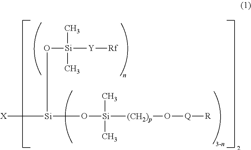
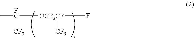
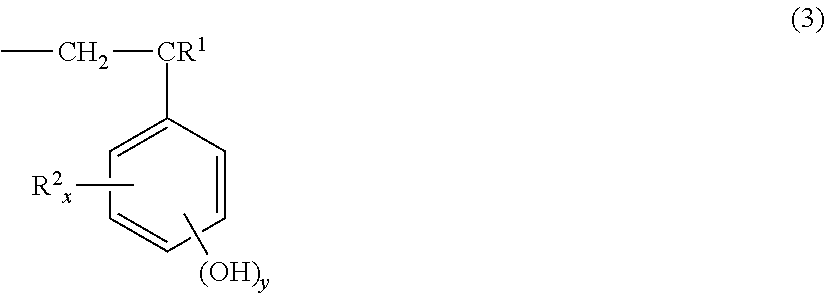
A chemically amplified positive resist composition comprising (A) a substantially alkali insoluble polymer having an acidic functional group protected with an acid labile group, (B) an acid generator, and (C) a perfluoroalkyl ethylene oxide adduct or a nonionic fluorinated organosiloxane compound is coated, exposed to UV radiation having a wavelength of at least 150 nm, and developed. The composition has advantages of uniformity and minimized edge crown upon coating, and no scum formation after development.
Description
CROSS-REFERENCE TO RELATED APPLICATION[0001]This non-provisional application claims priority under 35 U.S.C. §119(a) on Patent Application No. 2011-008942 filed in Japan on Jan. 19, 2011, the entire contents of which are hereby incorporated by reference.TECHNICAL FIELD[0002]This invention relates to a resist composition which is exposed to UV radiation having a wavelength of at least 150 nm (near and deep-UV regions) and developed without leaving residue, known as “scum”, and a pattern forming process. More particularly, it relates to a chemically amplified positive resist composition which is coated onto a substrate to form a relatively thick resist film of 5 to 100 μm thick, while improving coating uniformity and inhibiting a phenomenon that the thickness of resist coating is extremely increased at the periphery of the substrate, known as “edge crown” phenomenon.BACKGROUND ART[0003]The resist material for use in the microfabrication of semiconductor integrated circuits is required...
Claims
Login to View More Application Information
Patent Timeline
 Patent Type & AuthorityApplications(United States)
IPC IPC(8): H01L21/3205G03F7/20G03F7/039
CPCG03F7/0046G03F7/0048G03F7/0757G03F7/0755G03F7/0392Y10S430/1055
InventorYASUDA, HIROYUKITAKEMURA, KATSUYAKOIKE, NORIYUKI
OwnerSHIN ETSU CHEM IND CO LTD