Method for smart defect screen and sample

a defect detection and defect technology, applied in the field of defect diagnosis, can solve the problems of reducing the sample count of review samples, affecting product yield, and reducing the relevant product yield, so as to improve the systematic defect capture rate and defect review efficiency

Active Publication Date: 2012-07-19
ELITETECH TECH
View PDF9 Cites 19 Cited by
  • Summary
  • Abstract
  • Description
  • Claims
  • Application Information

AI Technical Summary

Benefits of technology

[0007]The invention provides a method for smart defect screen and sample to improve the systematic defect capture rate and defect review efficiency.
[0009]Therefore, the method for smart defect screen and sample is capable of improving the systematic defect capture rate and reviewing efficiency under lower sampling-rate.

Problems solved by technology

During the fabrication process, the random particle defect and systematic defect are affecting the product yield.
As the feature size of the design layout shrinks, the product yield relevant defects become smaller.
Further, when a scanning electron microscope (SEM) review tool is used to observe and classify all killer defects in order to determine a potential clue, a limited time in the fab and Review SEM capacity may restrict review sampling count per wafer.
Consequently, it may be difficult to identify a defect of interest type that should be monitored in production and have increased risk of missing the killer defects.
Without a quick and innovative method to identify systematic defect early, fab may suffer larger yield loss and take longer learning curve cycle time toward volume production.

Method used


Image

  • Method for smart defect screen and sample
  • Method for smart defect screen and sample
  • Method for smart defect screen and sample

Examples


first embodiment

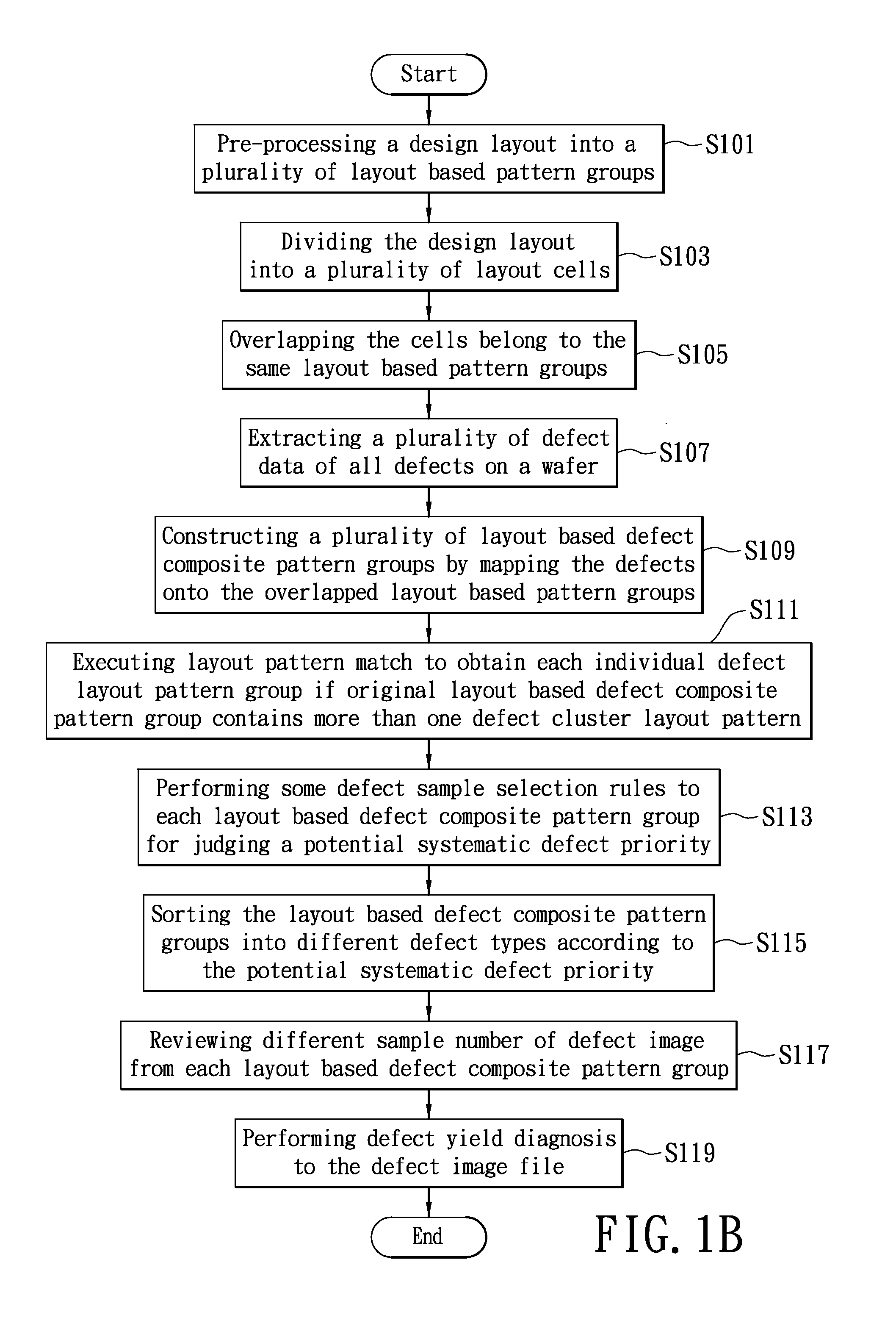
[0023]FIG. 1B shows a flowchart of the method for smart defect screen and sample in accordance with the present invention.

[0024]Please refer to FIG. 1B and associated with FIG. 1C. The FIG. 1C illustrates a schematic view of the method for smart defect screen and sample in accordance with the first embodiment of the present invention.

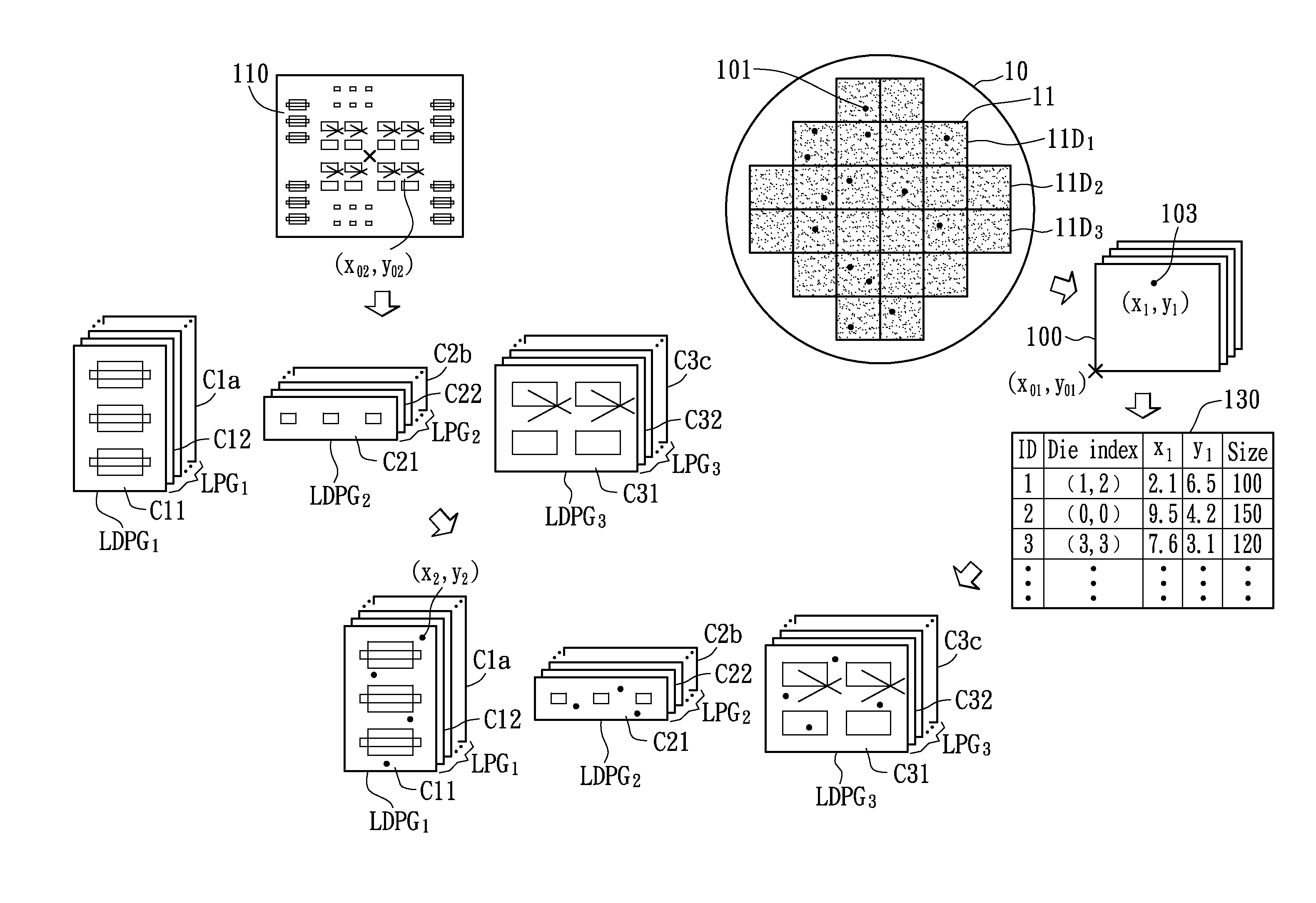
[0025]The user pre-process a design layout 110 into a plurality of layout based pattern groups (S101). The design layout 110 is designed for the wafer 10 by the user. The wafer 10 has a full-chip layout 11 on it and the full-chip layout 11 includes a plurality of dice 11D1, 11D2, and 11D3. The computer extracts a design layout 110 of each die 11D1, 11D2, or 11D3, in the full-chip layout 11 from a design layout database (not shown). The design layout 110 has a plurality of layout patterns and a second reference point (xO2, yO2) at the center of the design layout 110 or the wafer 110. The layout patterns have different layout pattern features.

[0026]The co...

second embodiment

[0039]FIG. 2 shows a flowchart of the method for smart defect screen and sample in accordance with the present invention.

[0040]Referring to FIG. 2, the second embodiment is similar to the first embodiment, while the difference between the method for smart defect screen and sample of the second embodiment and the first embodiment is that after constructing a plurality of layout based defect composite pattern groups LDPG1, LDPG2, and LDPG3, etc (S109) in the first embodiment, the second embodiment further comprises following steps.

[0041]The computer performing some defect sample selection rules to each layout based defect composite pattern group LDPG1, LDPG2, or LDPG3, etc for judging the potential systematic defect priority. The defect sample selection rules comprise calculating the hit rate of each layout based defect composite pattern group LDPG1, LDPG2, or LDPG3, etc (S211). The hit rate may be associated with the defects count and the cell number of each layout based defect compo...

third embodiment

[0051]FIG. 3 shows a flowchart of the method for smart defect screen and sample in accordance with the present invention.

[0052]Referring to FIG. 3, the third embodiment is similar to the first embodiment, while the difference between the method for smart defect screen and sample of the third embodiment and the first embodiment is that after generating the defect pattern library and the defect yield report by performing defect yield diagnosis to the defect image file (S119), the third embodiment further comprises following steps.

[0053]The design house 30 downloads the defect pattern library from the web site of the fab 20 through internet (S321). The designer in the design house 30 extracts a new design layout from the design layout database in the computer (S323). The computer performs the pattern match between a plurality of new design layout patterns and the layout patterns in the defect pattern library (S325).

[0054]The computer identifies a location of a potential systematic defe...


PUM


Abstract

A method for smart defect review is disclosed. The method includes pre-processing a design layout into a plurality of layout based pattern groups, dividing the design layout into a plurality of cells, overlapping the cells belong to the same layout based pattern groups, extracting a plurality of defect data of all defects on a wafer, constructing a plurality of layout based defect composite pattern groups, executing layout pattern match to obtain each individual layout based defect composite pattern group, performing some defect sample selection rules to each layout based defect composite pattern group, sorting the layout based defect composite pattern groups into different defect types, obtaining a defect image file by reviewing different sample number of defect image from each layout based defect composite pattern group, and generating a defect pattern library or a defect yield prediction by performing a defect yield diagnosis to the defect image file.

Description

BACKGROUND OF THE INVENTION[0001]1. Field of the Invention[0002]The present invention relates to a method for defect diagnosis, and particularly to a method for defect screen and sample.[0003]2. Description of Prior Art[0004]The fabrication process for integrated circuit dice includes film deposition, masking, photo lithography, etching, etc. During the fabrication process, the random particle defect and systematic defect are affecting the product yield. The product yield is related to the die cost.[0005]As the feature size of the design layout shrinks, the product yield relevant defects become smaller. Fab has to increase the sensitivity of a scan and inspection tool in order to capture all killer defects on the wafer. As a result, the number of detected defects may increase and the percentage of non-killer defects may be higher. Further, when a scanning electron microscope (SEM) review tool is used to observe and classify all killer defects in order to determine a potential clue, ...

Claims


Application Information

Patent Timeline
Patent Type & Authority Applications(United States)
IPC IPC(8): G06F17/50
CPCG03F1/84G06F17/5081G03F7/7065G06F30/398
Inventor LEU, IYUNLIN, CHIN HSEN
Owner ELITETECH TECH
Why Eureka
Try Eureka